





New nanomaterial films incorporate conductive network and printed electromagnetic structures to provide broadband shielding for electronics, thus providing an alternative for traditional thicker materials.
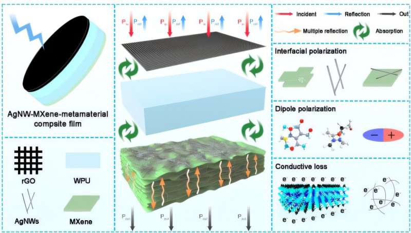
Scientists from the Hefei Institutes of Physical Science (HFIPS) under the umbrella of the Chinese Academy of Sciences (CAS) have created thin and flexible EMI shielding films that can block electromagnetic signals by 102.31 dB. By integrating interconnected nanomaterial networks and printed conductive structures, the new shielding material blocks the propagation of electromagnetic waves in a broad frequency band. At the same time, the scientists’ method allows producing the films on the square meter level, which is the problem of creating light shielding materials for electronics.

The technology incorporates the concept of the cross-dimensional percolation (CDP), whereby nanomaterials of different dimensions create a three-dimensional interconnected conductive network. In particular, the researchers employed 1D AgNWs and 2D MXenes to create the conductive network. This structure provides pathways for the transport of electrons and phonons and spaces for multiple reflection and absorption of electromagnetic waves.
To enhance the effectiveness of shielding, the team embedded the film with precisely printed metastructures in the form of graphene-based meshes. They play a role in managing the interactions between electromagnetic waves through impedance matching and enhancing the frequency range as compared to single-material shielding structures. The study showed a shielding efficiency of 102.31 dB in the frequency range of the X-band.
Fabrication includes three major steps: pressure filtration, precise inkjet printing and transfer process. The team optimized the material composition and created an ink with special conductive properties. Surface chemistry modification tackled the brittleness issues related to the composite films, making them foldable.

This development helps overcome the drawbacks of traditional EMI shielding materials that require extra thickness for effective protection. They also have a limited frequency range. This technique combines several electromagnetic attenuation mechanisms in one material system, such as conductive loss, dipole polarisation, and interfacial polarisation.
This research can be utilized to create protection against EMI in wearable electronics, delicate electronic gadgets, communication devices, and other similar uses where shielding of a thin, flexible nature is required. It also provides a way of creating large electromagnetic control films.