





Researchers have uncovered the physics behind radiation-induced semiconductor failure, opening possibilities for designing more resilient electronic devices for space exploration, nuclear energy and other extreme environments.
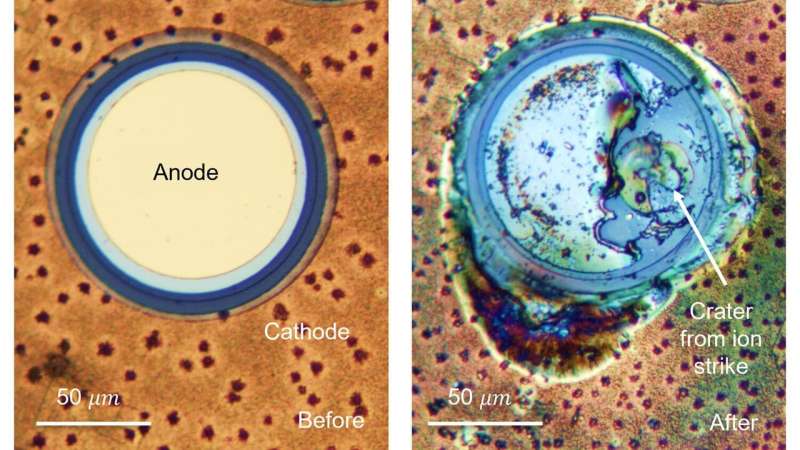
Scientists from North Carolina State University have come up with a theoretical physics model that helps understand why semiconductor devices are subject to catastrophic failure due to irradiation with energetic particles. This discovery may be used in order to build radiation-resistant electronics for application in nuclear power stations, space missions, fusion reactors, and medical devices.

This study is concerned with the phenomenon called single-event burnout (SEB) that refers to the process in which a single energetic particle leads to damage in an electronic device running on high voltage. Engineers were able to measure the maximum voltage at which such a failure may occur, but they could not explain its physical nature.The study considered SEB in aluminum nitride (AlN) that is ultrawide-bandgap semiconductor and can be used in electronics in high-power and high radiation environment due to the possibility of its operation at high electric fields.
In their research, the scientists considered AlN diodes irradiated by heavy ions. Passing through a semiconductor, an ion produces charged particles inside. At the application of an electric field to the diode, separation of positive and negative charges occurs and results in the formation of a high electric field at the path of a particle. Once this local electric field becomes large enough, an electron avalanche occurs. As a result, there is an immediate energy release, causing catastrophic physical damage, thus making the device useless due to a phenomenon called single event burnout.
To describe this phenomenon, the scientists used their experimental data in addition to data obtained from other semiconductors and computer simulations. Thus, they have managed to construct a mathematical model that describes the physics behind SEB for different devices and semiconductors. It was found that the semiconductor AlN can endure much larger electric fields before the SEB phenomenon occurs in comparison with some other semiconductors. The researchers pointed out that, as compared to applied voltage, it is the electric field strength which allows comparing semiconductor materials. Such results would provide design criteria to enhance the resistance of semiconductors to radiation damage. Understanding the way local electric fields cause failure in the devices would help engineers to alter the characteristics of materials and designs to prevent device failure.