


We are moving to a world which wants everything small except profits. We have small computers on our wrists, which we smartly call a smartwatch. Then we have the smart glasses, which somehow incorporate wireless transmitters in the sleek frame. This trend is spreading throughout technology. We have reached a level of fabrication, never seen before. We seem to want smaller processors, smaller chips, smaller devices, but we somehow seem to misplace our keys everyday.
Things going small every day
Suppose you want to buy a system, that could efficiently work multiple apps at the same time. You could either go for a desktop with multiple units, with separate central processing unit (CPU), monitor, keyboard, mouse and other peripherals. However, you have the other nifty option of going for a laptop. It is light, it is portable and the best of all, it does all that you want it to do. Is this really a competition?

We seem to go for smaller devices. These can be handled easily, at our own leisure and get the job done. You had the option to go for the desktop, but you went for the laptop. It performs the same tasks with the added benefit of a smaller form factor. All the parts inside a desktop have an even smaller versions of them, build with portable devices in mind. These are similarly efficient and look sleek as well. Assemble them together and you have a sweet deal with a personalised machine.
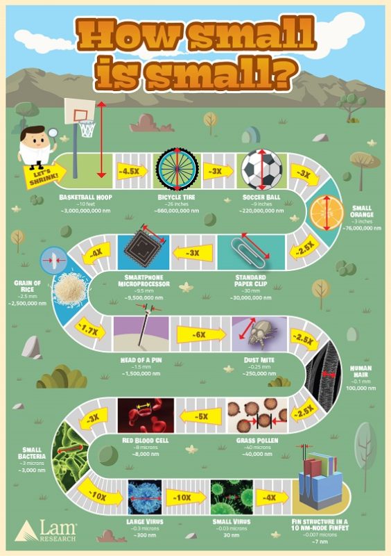
How small is small
The below infographic from Lam Research has a very interesting take on the size of technology at present.
How is it inside the chip?
One of the most astounding aspects of semiconductor chips is their incredibly small scale. Practically measured in atoms, some feature dimensions are on the order of nanometers (nm) – that’s one billionth of a meter and more than 10,000 times smaller than the size of objects that can be seen with the naked eye.
Most microprocessors today measure 10 nm as the shortest distance between gates. But seven nm distances are expected to be available by 2018, with five nm following closely in the near future. Last year itself, fabrication of 5 nm test chips was done by IMEC and Cadence. The chips might not be fully functional devices, but just to evaluate patterning. Nevertheless, it’s here.
FinFET transistors are moving to replace planar, resistive memory technologies just as Resistive random-access memory (ReRAM) plans to succeed NAND Flash and Synchronous dynamic random-access memory (SDRAM). With increasing fabrication standards, these will soon become the norm.
Sizing up the current FinFET
Starting from 22 nm, 10 nm Fin Field Effect Transistors (FinFETs) are expected to be available by the end of this year. Foundry vendors are battling each other for fabrication of 16/14nm designs, however the migration to finFETs is expected to be slow and expensive. This is in part due to the constant migration to the newer 10 nm which is expected in the market by the end of the year.
The pricing with the newer 10 nm model expected to be about 4 times the earlier 28 nm planar chip. At such high production cost only the foundries with very high volume can afford to produce this next generation chip. Also there are expected to be various complex tradeoffs in terms of circuit performance, circuit areas and options available to the designers.
Challenges in 10nm fabrication
One of the biggest question for adoption would be economics. Cost is one of the most significant factors. According to Gartner, the average integrated circuit (IC) design cost for a 28 nm planar chip amounted to about 30 million USD. This doubles when we move up to the current 14nm designs. However, all this is left in the dust, when we talk about 10 nm, which costs upwards of 120 million USD. Add to that the amount of man hours put into the development, it becomes an entirely different battle.
Another question can be the support by electronic design automation (EDA) tools for 10 nm. Can the current EDA tools account for all of the different possible unknowns? Which makes the big question to be if the power, performance and cost at 10nm better than 14 nm? If yes, how significant is the advancement?
Such uncertainty in the 10 nm however does not seem to haze development. It would be interesting to note how far can we scale FinFETs.
Going one size down
The 7 nm finFET is expected to be a revolutionary improvement. According to some industry experts, we can develop the 10 nm chips using the currently silicon germanium mix. However to take it a step further we might have to think about a new material, possibly a more complex germanium mix could come to the rescue.
When going down to such levels, another matter that comes up is that the fin width would be nearing its limit at about five or six nm. The lithography rules are expected to be pushed to the limits, as the biggest challenge is expected to be multiple patterning. According to Gartner, this would be upwards of 160 million USD, which would make it more than 5 times to produce a 28 nm planar chip.
Nano electronics could be the next thing
The current smartphone weighs inwards of 200 grams, and that’s the heavy one. It is certainly not lifting weights at the gym but imagine a further reduction in weight. Nanotechnology holds some answers for you. Last month we had a nanotechnology based battery concept that would run at 90% capacity even after a million recharge cycles. And that’s just the beginning.
Some of the nanoelectronics areas under development would be the displays on electronics devices. Reducing the power consumption, weight and thickness of the screens would increase the battery life. Advances in memory design are also underway. We could very well see memory chip with a possible density of one terabyte in an inch or so.

I have a mini project to do .so i want a simulation circuit for that can you please help me by providing that .
Hi Dinesh,
We have a dedicated category for projects.
It can be found at: circuits/code (link embedded) section of our website.
Hope you find what you are looking for.
For further enquiries, you can send an email to [email protected]
Please share your mini project at [email protected].