




Texas Instruments has developed a reference design for generating a low-ripple 1.2 V supply from a wide 3.8 V to 30 V DC input range.
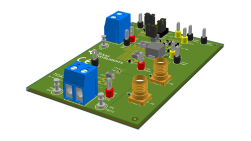
Texas Instruments has developed a low-ripple power supply reference design for applications that require a clean and stable 1.2 V supply. The design accepts a DC input voltage ranging from 3.8 V to 30 V and provides up to 3 A of continuous output current, with a maximum output power of 3.6 W.
The reference design uses a synchronous buck converter followed by a second-stage LC filter to reduce output ripple. It is specified to provide less than 1 mV peak-to-peak output ripple. The converter uses peak-current control with internal compensation and is designed for applications where low power-supply noise is important.
The design is intended for communications and data-centre equipment, including active antenna system intermediate-frequency sampling and optical datacom modules. Its low-ripple output can support analogue and mixed-signal circuits such as analogue-to-digital converters and analogue front ends, where supply noise can influence system performance.
Texas Instruments specifies an operating junction-temperature range of –40°C to 150°C for the design. The reference design provides a practical platform for evaluating the low-ripple power supply architecture across its specified input-voltage and output-current ranges.
Texas Instruments provides supporting resources for the reference design, including a design guide with verified performance data, bill of materials, assembly drawing, computer-aided design and engineering (CAD/CAE) files, Gerber files, PCB layout and schematic. The fully assembled board is intended for testing and performance validation and is not available for sale.
For more information, click here.

