


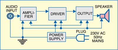
 Here we put all the theory to work and present a simple 1.5W power amplifier module that can be easily built with readily available components. The block diagram of the amplifier is shown in Fig. 1. It is typical of most audio amplifiers, although the circuit is somewhat different.
A power amplifier contains audio input, amplifier, driver, output and power supply sections. The amplifier section provides most of the voltage gain. The driver stage is a buffer between the amplifier section and the output stage.
The output stage usually has to drive a low-impedance load such as a loudspeaker. The power comes from the power supply, and the output signal appearing across the load should ideally be a replica of the input signal. In other words, the output stage takes power from a DC supply to boost the signal so it can drive a load.

Power Amplifier Circuit Description
The circuit shown in Fig. 2 shows the amplifier, driver and output sections. The amplifier section is built around JFET VHF/UHF amplifier 2N5484 (T1) and NPN transistor BC548 (T2). The driver section is built around transistor BC639 (T3) while the output section is built around transistors BD139 and BD140 (T4 and T5).
The input signal is coupled to volume control VR1 via capacitor C1. The value of VR1 is specified as 1-megaohm. Since the gate terminal of FET (T1) can be regarded as an open circuit, the input impedance of the circuit is equal to the value of VR1.
Like all audio volume controls, VR1 needs to have a logarithmic taper (usually denoted as ‘type C’) to give an apparent linear relationship between rotation of the control and the volume level. This is necessary because human hearing follows a logarithmic response, in which a change in the output power by a factor of 10 is heard as a change by a factor of two.
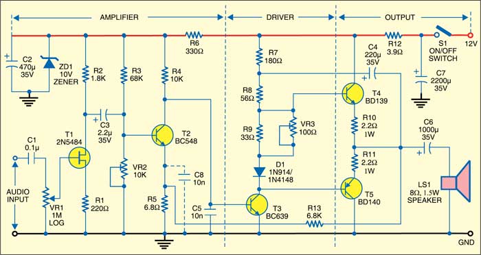
The FET stage in the amplifier section is used to give a high input impedance. The next stage is common-emitter amplifier comprising transistor T2. Preset VR2 is used to adjust amplification and avoid direct coupling between transistor stages T2 through T5. This means that DC voltages for T3, T4 and T5 are all determined by the collector voltage at T2.
The most important voltage is at the emitters of T4 and T5. Preset VR2 is used to adjust this to half the supply voltage.
To stabilise this and other voltages in the circuit, resistor R13 gives negative feedback from the output to the emitter of transistor T2. If capacitor C8 is not included, the feedback will be for both DC and AC voltages. It will be for DC only if C8 is added.
When voltage at the emitters of transistors T4 and T5 rises, say, due to a temperature change, the voltage at the emitter of transistor T2 will also increase by way of R13. This will cause T2 to conduct less current, making the DC voltage at its collector increase. As a result, transistor T3 will conduct more current and its collector voltage will drop. This then reduces the voltages at the bases of T4 and T5 and hence their emitter voltages.
Driver transistor T3 and its collector load is the base circuitry associated with T4 and T5. In effect, T3 is connected as a common-emitter amplifier. The output signal developed across T3 is applied to the base of T4 via diode D1 and the parallel combination of resistor R9 and preset VR3. The base of PNP transistor T5 connects directly to collector of T3.
The driver stage therefore drives a relatively low-resistance load, requiring a transistor capable of handling high power.
The output transistors are NPN transistor T4 and PNP transistor T5, connected as a complementary symmetry class-AB output stage. In this configuration, an NPN transistor and a PNP transistor (complementary) with equal current gains (symmetrical) are required. Thus, ideally, the DC current gains of T4 and T5 should be matched by measurement.
The DC biasing circuit for T4 and T5 has one diode and two parallel-connected resistors. Preset VR3 is used to adjust the quiescent collector current of T4 and T5 and therefore the class of operation.
The output stage also involves capacitor C4, which is known as a bootstrapping capacitor. Bootstrapping is included to allow a higher output voltage swing. If capacitor C4 is not included, biasing resistors R7 and R8 are combined into a single resistor.
Ideally, the output signal should be able to swing from 0V to the value of the supply voltage. However, this cannot happen due to the 0.6V forward bias required across the base-emitter junctions of the output transistors and also the losses. For the positive half cycle, if the output is to reach the supply voltage, the voltage at T4 must be at least 0.6V higher than the supply voltage. Similarly, an output of 0V can be obtained only if the base voltage of T5 falls to –0.6V.
By adding bootstrapping capacitor C4, the output voltage swing is effectively added to the DC bias voltages. Thus, for the positive half-cycle, the positive change adds to the bias voltage at T4, causing it to conduct more current and produce a higher output voltage. Similarly, in the negative half-cycle, the negative-going swing reduces the quiescent bias voltage, helping T5 turn on harder and produce a lower output voltage.
An important aspect of amplifier design is power supply decoupling. When the output stage is producing full output power, the power supply delivers substantial peak currents. Under these conditions, it is possible that some of the audio signals appear on the supply line.
To prevent this signal from affecting the operation of the rest of the circuit, it must be eliminated from that part of the supply feeding the voltage amplifier section. So resistor R6 is added together with C2 and ZD1 to maintain the amplifier’s supply voltage to a constant 10V.
Assemble the circuit on a general-purpose PCB and enclose in a suitable cabinet. Mount the diodes, electrolytic capacitors and transistors with the correct polarity. Output transistors T4 and T5 have a metalised surface on one side, which should face the centre of the board.
A heat-sink is required for both the transistors. Either a small (20mm2) piece of aluminium or a commercially available heat-sink can be used.
The heat-sinks on T4 and T5 should be insulated from the transistors with a piece of Mylar or similar material, as this transistor (and therefore the heat-sink) connects directly to the power supply.
Important Points to Remembers Before Testing the 1.5W Power Amplifier
Before applying power to the circuit, connect an 8-ohm load (resistor or loudspeaker) to the output, and capacitor C1 between the input terminal and the volume control. Set the volume control to minimum and then apply power—either from the plug pack or an external 12V DC supply.
Ensure that both the output transistors are cool when touched. If not, try adjusting preset VR3. The correct setting for VR3 should give a quiescent collector current of around 100 mA through T4 and T5.

This Amp is ideal for my project ( vintage table top radio circa 1965 repair for a friend). Is there available for this circuit a black and white track layout as I do not have the equipment to do the artwork?
Regards Mo K