
The custom-built matrix display for primary school children’s character visualisation is an accessible innovation that strengthens primary education. Its 8×8 programmable format offers a seamless and dynamic platform for young learners to visually recognise and understand alphabets and numbers, supported by user-friendly programmability.
POC Video Tutorial
By integrating modern technology into the classroom, the system delivers an economical learning solution without straining resources, owing to its low-cost design. This approach deepens understanding of language and characters while sparking curiosity through an effective blend of technology and education.
The matrix display also paves the way for a more engaging and effective learning experience, helping primary school students progress confidently in character recognition and literacy development.

Transforming the approach to elementary education, the 8×8 programmable matrix display serves as an innovative and engaging teaching aid for character visualisation. The system creates a dynamic and visually appealing platform through which children can explore and understand characters more effectively. By seamlessly combining technology with learning, it stimulates curiosity while fostering a deeper understanding of language and letter formation.
As modern educational technologies continue to evolve, this teaching aid paves the way for a more interactive and effective learning experience, supporting primary students in their journey of literacy development and character recognition.
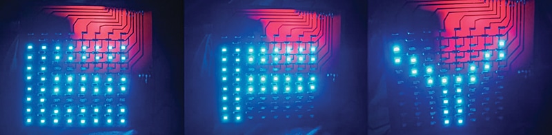
This LED matrix can generate multiple patterns using an Arduino program based on high and low logic levels. Fig. 1 shows the finished system along with a sample output displayed as an EFY light illusion on the 8×8 LED matrix. The circuit can be powered using a 5V DC supply. The components required for this system are listed in the Bill of Materials table.
| Bill Of Materials | ||
| Name | Specification | Quantity |
| Arduino Uno | Board | 1 |
| SMD LEDs | 1206 package | 64 |
| SMD resistors | 1206, 1kΩ | 8 |
| SMD resistors | 1206, 0Ω | 56 |
| FR4 PCB board | 10cm×10cm | 1 |
| Male-to-male jumper wires | — | As required |
| Single-pin connectors | — | As required |
| Wires, solder wires | Soldering iron | As required |
Circuit and working
The matrix display is arranged in rows and columns and interfaced with the Arduino Uno. The columns are connected to the cathodes of the LEDs, so a column must be set low to enable an LED, while the rows are connected to the anodes and must be set high to turn on a specific LED.
If both the row and column of an LED are at the same level (either high or low), there is no potential difference across the LED, and it remains off. Thus, to control a particular LED, its row is set high and the corresponding column low. Fig. 2 shows the circuit connection of the 8×8 SMD matrix display interfaced with the Arduino Uno.
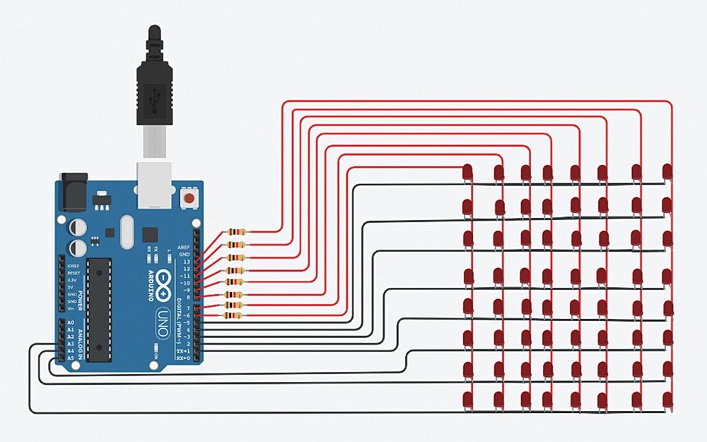
To control multiple LEDs within a row, the row is kept high while the required columns are set low. Each column can be driven high or low depending on the desired LED state; a high level turns the LED off, while a low level turns it on (active-low configuration). By selectively controlling the column states, multiple LEDs within a row can be operated simultaneously.
The system is programmed using the Arduino Uno, a widely used microcontroller board based on the ATmega328P, suitable for controlling LED matrices and other embedded applications. The Arduino IDE is used to write, compile, and upload the code to the board.
While writing the code, pins are assigned for rows (R1-R8) and columns (C1-C8). In the setup() function, all row and column pins are configured as OUTPUT. The following functions are then defined:
- on_row. Turns on a specific row by setting the corresponding row pin high
- on_column. Turns on a specific column by setting the corresponding column pin low
- off_row. Turns off a specific row by setting the corresponding row pin low
- off_column. Turns off a specific column by setting the corresponding column pin high
- off_all. Turns off all rows and columns of the LED matrix by calling the offr and offc functions for each row and column pin
A delay function (delay(t)) is introduced to provide a time gap between steps, helping to control the display timing.
Construction and testing
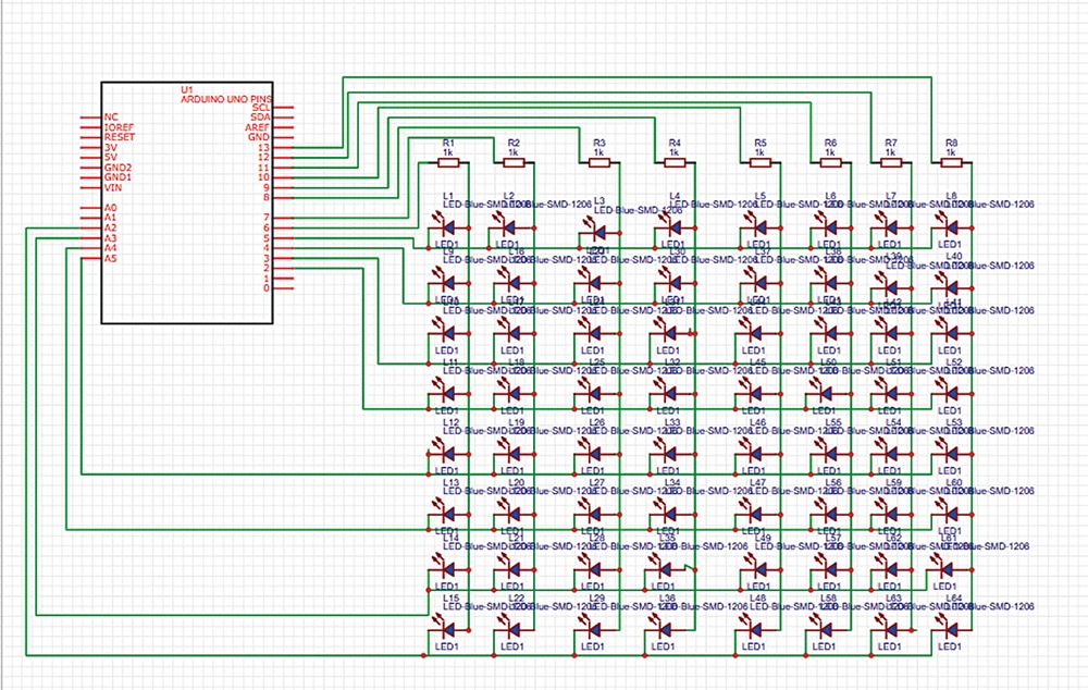
The 8×8 matrix display interfaced with the Arduino Uno is constructed using 64 SMD 1206 LEDs and 1kΩ resistors. To avoid the intersection of circuit lines, 0Ω resistors are used. Fig. 3 shows the circuit diagram of the 8×8 SMD matrix display interfaced with the Arduino Uno.
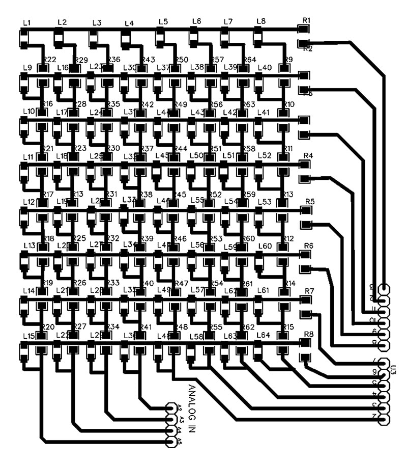
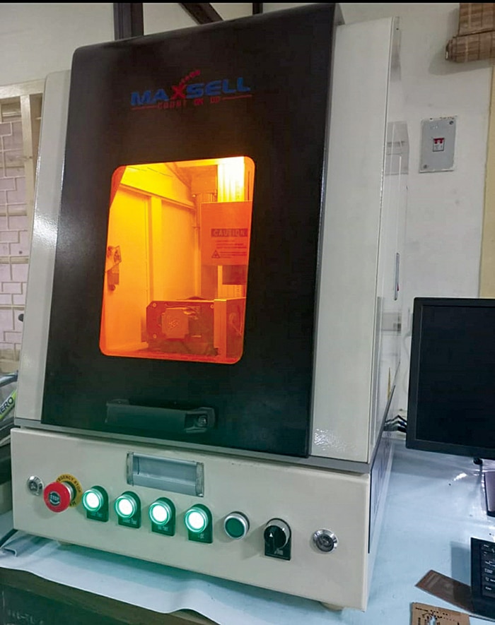
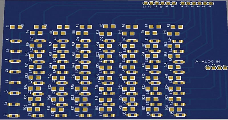
The first stage in developing the SMD PCB for the 8×8 matrix display involves designing the PCB layout using EDA software. The layout is then exported as a PNG, as shown in Fig. 4, and imported into EzCAD for laser etching on an FR4 board. Using a laser etching machine, the bare PCB for the matrix display is fabricated, as shown in Fig. 5.
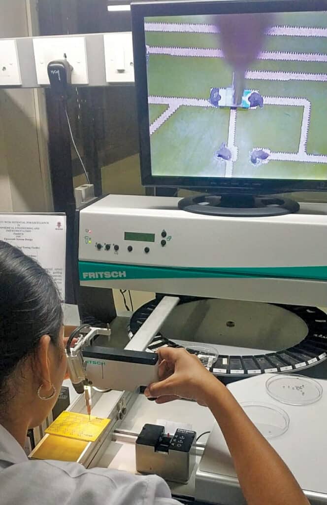
The second stage involves assembling the components. After cleaning the etched board, a generous amount of solder paste is applied to the solder pads. Using a pick-and-place machine (see Fig. 6), the components are then mounted in their corresponding positions.
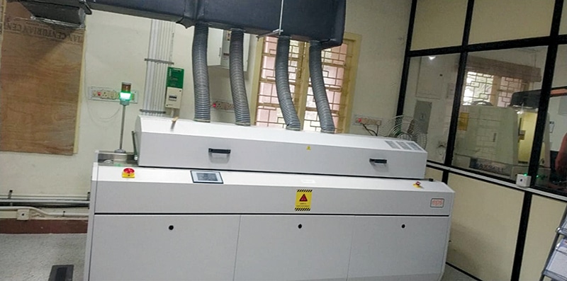
The final stage of PCB fabrication is soldering. In this stage, a reflow oven is used to solder the components using the hot-air reflow method. The five chambers of the reflow oven (see Fig. 7) are set with progressively increasing temperatures and controlled airflow to ensure a proper soldering finish.
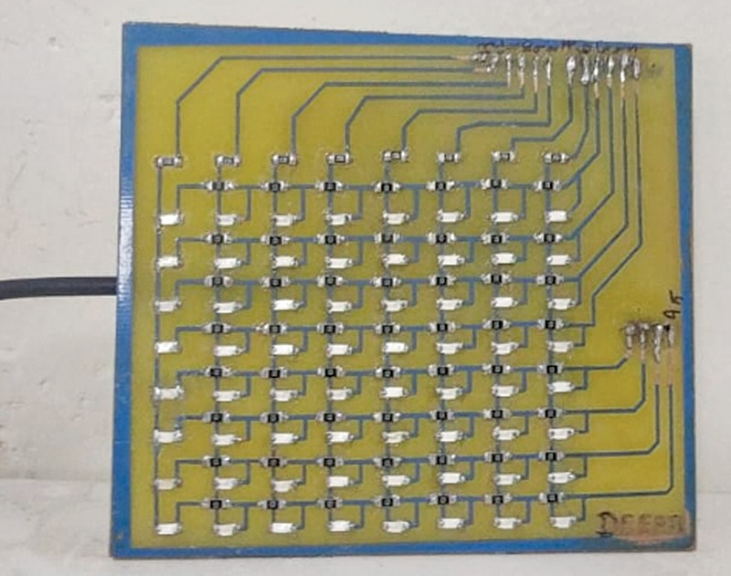
Male-to-male connectors are hand-soldered for interfacing with the Arduino Uno. After completion of the soldering process, the circuit should be carefully inspected to ensure there are no short or open connections. Once verified, the PCB is connected to the Arduino and the program uploaded to visualise the output. Fig. 8 shows the author’s PCB prototype, while Fig. 9 illustrates the actual-size 3D model of the board.
Deepti Rekha S.A. is an M.E. graduate and a Ph.D. scholar at the College of Engineering Guindy, Anna University. Currently a Junior Research Fellow at the Society for Electronic Transactions and Security (SETS), her research interests include PCB Design and Hardware Security. This project was conducted under the guidance of Dr N. Ramadass, a faculty member in the Department of Electronics and Communication Engineering at Anna University.