


 This circuit breaker employs a single operational amplifier (op-amp) and yet has a wide range and is user-friendly. A circuit breaker is an electrical switch intended to protect an electrical circuit or device from damage caused by excess current flow or short-circuit. A basic circuit breaker includes a simple fuse and a normal miniature circuit breaker (MCB). It is designed for a fixed-rated current value in terms of amperes.
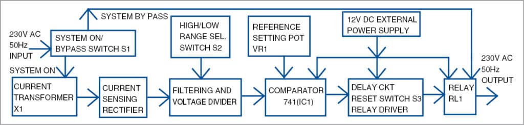
In this circuit, you can select the current value range from milli-amperes (mA) to a few amperes. A simple circuit compares current with a preset value. If current increases beyond the preset value, the circuit breaks (opens) the current flow to the load. The circuit then automatically closes and restores after a specified time or manual reset. The block diagram of the circuit breaker is shown in Fig. 1.
Circuit and working
The circuit diagram of the adjustable AC circuit breaker is shown in Fig. 2.
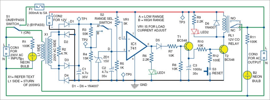
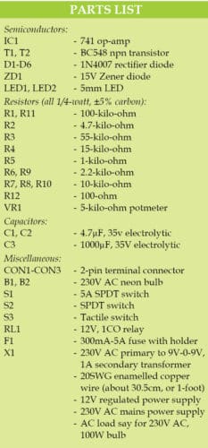
It is built around transformer X1, six 1N4007 diodes (D1 through D6), one 741 op-amp (IC1), two LEDs (LED1 through LED2), two npn transistors BC548 (T1 and T2), 15V Zener diode ZD1, 12V-1CO relay and a few other components.
The circuit is constructed around the 741 op-amp. The op-amp is used in non-inverting comparator mode.
Major construction lies in the design of the current transformer as explained below. Take 230V AC primary to 9V-0-9V, 1A secondary transformer (X1) as shown in Fig. 3.
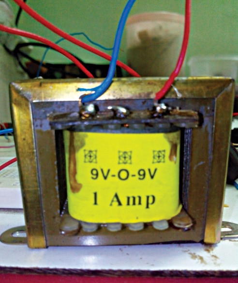
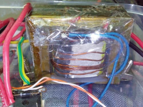
In this transformer, usually low-voltage secondary winding is wound around 230V AC primary winding. X1 has 230V AC primary (say, 230V AC side) and 9V-0-9V, 1A secondary, but here secondary winding is unused (need not be removed). A few turns (three to five) of 20SWG enamelled copper wire, say L1, is wound on top of the winding (around its bobbin), as shown in Fig. 4.
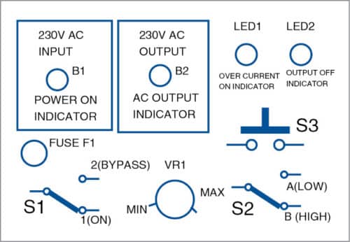
Switch S1 is an on/bypass switch. You can bypass the circuit breaker system by keeping S1 towards position 2 (bypass), where load current flows directly to AC output through fuse F1. Here, F1 acts as a traditional protecting device.
If S1 is at position 1 (on), load current flows through L1 winding of X1 and relay RL1 contacts, to AC output connected to AC load.
Load current is passed through L1, and is used for load current measurement. Voltage produced at 230V AC side of the transformer is proportional to the amount of load current passing though L1 winding of X1. Voltages corresponding to the load current flowing through winding L1 are listed in Table I. Values may vary depending on number of turns and value of R2.
Output of 230V AC side is rectified using a bridge rectifier. Resistor R2 limits the voltage developed at 230V AC side of X1. Rectified voltage is filtered and connected to R3 and R4.
Capacitor C2 is used for further filtering input voltage at point D (pin 3 of op-amp). ZD1 is used as a protective device for suppressing voltage beyond 15V during unusual conditions. LED2 is connected in parallel with the relay, and is used to indicate device off or circuit open status. LED1 is connected at output pin 6 of IC1. It is used to indicate output sense. It is also used for setting load current.
When load current is more than the set value, LED1 glows. Two neon bulbs (B1 and B2) are used to indicate 230V AC input and AC output. AC output connector CON3 is used to connect the load.
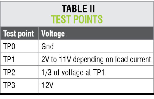
Test point TP1 provides DC voltage corresponding to load current. Two resistors (R3 and R4) are chosen to facilitate current measurement from a low value, that is, 300mA, to a high range of 5A. Developed voltages at TP1 and TP2 corresponding to current via L1 winding are given in Table II.
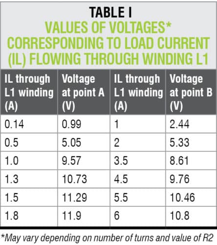
TP1 and TP2 are connected to points A and B of SPDT switch S2. Its middle pin D is connected to pin 3 of IC1. S2 is a range-selection switch. When it is at position A, low range is connected to pin 3 of IC1. When it is at position B, high range is connected to pin 3 of IC1. Table I shows the voltage developed during load current.
Voltage at pin 3 of IC1 acts as comparing voltage. Potmeter VR1 provides the reference voltage for comparison, which varies from 2V to 11V. VR1 is used for load current adjustment. It is varied to set the reference voltage at point C (pin 2) of IC1. When voltage at pin 3 of IC1 exceeds set reference voltage at pin 2 due to current through L1, output at pin 6 of IC1 goes high and triggers relay RL1. Due to this, 230V AC output is switched off, and load current flowing through L1 is cut off.
A delay circuit is provided between IC1 and relay circuit. T1, C3 and R10 provide the delay. When output of IC1 goes high at pin 6, T1 conducts and charges C3 to maximum voltage (near 12V). D5 is used to pass the current in one direction, towards the base of T1.
C3 is discharged only through T2 via R10. T2 is used to drive RL1. R10 and C3 provide maximum delay of 10 seconds approximately. S3 is reset and connected to base of T2 through R12 to ground. When S3 is closed, it switches off T2, RL1 gets de-energised and its pole contact returns to its NC position.
Construction and testing
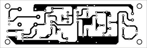
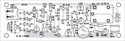
An PCB layout of the adjustable AC circuit breaker is shown in Fig. 5 and its components layout in Fig. 6.
Download PCB and Component Layout PDFs: Click here
After assembling the circuit on the PCB, connect external 12V across CON2. Note that, CON1 and CON3, S1, F1, and B1 and B2 are not included in the PCB. Connect these through external wires as per the current requirement of the load (device). Connect 230V AC across CON1 and load across CON3. Proposed front panel layout is shown in Fig. 7.
After assembling the circuit and before enclosing it in the cabinet, calibrate it as given below. Use a multimeter for measuring voltages and adjusting cutoff currents.
Calibration
- Keep S2 either at point A or B depending on load. For low current between 300mA and 1A, keep it at point A. For high current between 1A and 5A, keep it at point B.
- Keep current-adjustable VR1 to maximum anti-clockwise direction.
- Connect to 230V AC input at CON1 and load (device) across CON3. Keep S1 at point 1 to enable the circuit breaker.
- Use a multimeter to measure voltage at pin 3 of IC1.
- Using VR1, set voltage close to the voltage of pin 3 of IC1.
- Slowly rotate VR1 from maximum to minimum (clockwise) until LED1 glows and load gets turned off.
- Slowly turn VR1 slightly in anti-clockwise direction.
The circuit is now ready to use.
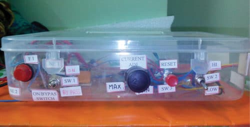
The author’s prototype is shown in Fig. 8.
Murali Krishna is working as junior engineer (telecom), BSNL, Rajahmundry, Andhra Pradesh. He is an electronics enthusiast, circuit designer and writer.

Excellent circuit breaker sir plz design small air circuit breaker in low cost 1amp up to range sir replace MCB or rccb elcb or some more things
Dear Sirs,
the download link for PCB and Component Layout PDFs seems to be incorrect.
Please can you fix this?
Kind Regards
Mitsos
Please refresh the page and retry
Dear Sirs,
the download link for PCB and Component Layout PDFs is incorrect.
The downloaded file pic-3-1.zip contains PCB and Component Layout PDFs of
Control Panel For Submersible Monoblock Pumpset project from January 2019 issue.
Please can you fix this?
Kind Regards
Mitsos
The file is correct, please recheck.