


 The principle of operation of this meter is based on pulse-width modulation. Larger the capacitance, higher is the pulse-width and vice-versa. The meter given here has one oscillator and two one-shot generators (OSG) built around RC components. An OSG is triggered by a free-running oscillator built around IC NE555 (IC1) The pulse-width of the OSG is determined by the capacitor under measurement (Cx). By passing the pulses from the OSG through a linear ammeter it is possible to measure its duty cycle. In other words, the deflection of the ammeter can be made equal to the duty cycle, which here becomes proportional to the value of the capacitor Cx due to linear property of the OSG time period.
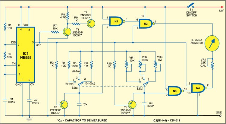
Fig. 1 shows the circuit diagram of analogue capacitance meter. The OSG comprises timing resistors (R4 through R6) and capacitor Cx, whose voltage is sampled by CMOS gate N1. Cx is discharged through transistor T3 connected in parallel. Cx is connected to pin 2 of gate N1. The voltage at pin 2 of gate N1 is used as the reference voltage to which Cx has to charge. Once this voltage is reached, the sampling gate output makes the transistion from high to low state, indicating the completion of the charging time. Charging time (on-time) of capacitor Cx is given by: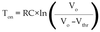
Here, Vo is supply voltage and Vthr is the threshold input voltage of gate N1. R=R4 through R6 and C=Cx. Due to this linearity of the RC circuit, a capacitor with twice the value would take twice the time. Thus the OSG pulse-width, and hence the duty cycle of the output waveform, becomes proportional to the value of the capacitor.

Due to stray capacitance of connecting wires the OSG does not pro-duce a zero pulse without capacitor Cx. To eliminate this, a similar auxiliary OSG, comprising presets VR1 through VR3 and a capacitor C3, is used. The presets VR1 through VR3 are adjusted such that for each range the meter gives zero indication when capacitor Cx is not connected. With these adjustments the meter is ready for use.
The oscillator built around IC1 should be configured such that its on-time period (TON) slightly exceeds the OSG on-time period (Ton) with the full range capacitor value and off-time period (TOFF) occurs just before complete discharge of capacitor. This becomes very important for capacitors having large capacitances.
The calibration of the ammeter is easy if suitable reference capacitor is available. It is recommended to per manently include a reference capacitor, say, 100nF. With a reference capacitor connected, you can easily set the calibration resistance using preset VR3 to obtain a full-scale deflection. This would finish the calibration for other ranges as well. The capacitance of Cx is given by the following expression: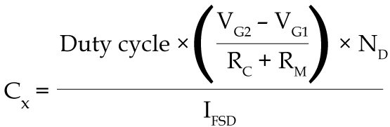
Here, VG2 and VG1 are the output gate voltages of N4 and N2, respectively. ND is the total number of divisions on the ammeter scale, RM and RC=VR3 are the meter and series calibration resistances, and IFSD is the full-scale deflection current of the meter.
The range of the instrument can be further extended by including lower valued range resistances (1kΩ gives 0-100nF and 100Ω gives 0-1µF). We have used a basic instrument to keep the diagram as simple as possible.
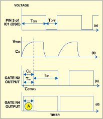
Since NE555 cannot supply the required current maintaining a constant voltage, additional driver stage of transistors T1 (2N3904) and T2 (N3906) have been included. The pulsed drive automatically cuts-off the supply during off-cycle, enabling a proper discharge of Cx, which is important to get the right value of the capacitor. Otherwise a partially charged capacitor will be subjected to the next charge cycle and indicate a lower value. An indicative timing diagram (not to scale) is given in Fig. 2.
The circuit takes some time to stablise thermally and is more suitable as a lab instrument. It is recommended to include a lower-valued variable resistance in series with the preset control-ling the current through the meter. This will allow easy frequent calibration of the instrument.
Assemble the circuit on a general-purpose PCB in a suitable enclosure. Approximately 63.5cm (25-inch) long test leads with crocodile clips are used for compensating the capacitance of C3. This capacitance can be changed according to the length of the test leads. Fix the ammeter in the front panel.
