




A compact buck converter design converts a wide input range to a low-voltage output while delivering 3 A in limited board space.
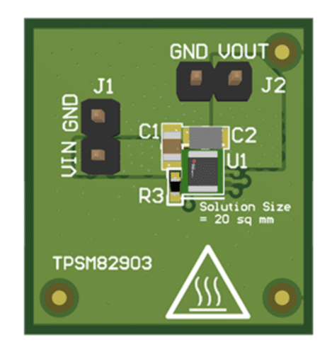
Texas Instruments (TI) has the TIDA-050055, a compact DC-DC buck converter reference design for applications where PCB space is limited. The design converts a 3 V to 17 V input into a 1.2 V output and can deliver up to 3 A of continuous output current. It uses a power module with an integrated inductor, reducing the number of external components needed in the power stage. The complete solution occupies about 20 mm², giving it a power density of 150 mA/mm².
The design is intended for applications such as smart locks and wearable devices, particularly battery-operated systems where low power consumption is important. TI has also listed data centres, wired networking, wireless infrastructure, factory automation and test and measurement among the possible application areas. The design operates across a -40°C to 125°C junction-temperature range and provides total system voltage accuracy of ±1% across this temperature range.
The wide input range allows the same design to work with 3.3 V, 5 V and 12 V supply rails, as well as single-cell and multi-cell lithium-ion battery systems. The reference design produces a 1.2 V output, with the specified output voltage ranging from 1.185 V to 1.215 V. The switching frequency is set to 2.5 MHz, while the typical operating quiescent current in power-save mode is 4 µA.
The converter uses a synchronous buck architecture with DCS-Control and supports 100% operation. One of the important design features is Automatic Efficiency Enhancement (AEE). Instead of maintaining a fixed switching frequency across the entire input and output voltage range, the converter adjusts its switching frequency while maintaining the required ripple current. This helps maintain efficiency when the input-to-output voltage ratio changes. The approach is particularly useful when converting a high input voltage to a much lower output voltage, where a fixed-frequency converter can experience a larger efficiency reduction.
The design also uses automatic PFM/PWM operation. At higher output currents, the converter operates in PWM mode. As the load decreases, it enters power-save mode when the inductor current becomes discontinuous. In this mode, the switching frequency decreases with load current to reduce switching losses. The transition between power-save and PWM operation is seamless as the load changes.
The output-discharge function is enabled in the reference design. It provides a defined downward ramp of the output voltage when the converter is disabled and keeps the output close to 0 V while the device is off. For faster startup, the soft-start pin is left floating, allowing the converter to use its programmed startup time.
The integrated 1-µH inductor is one of the main contributors to the small solution size. TI recommends a 22-µF output capacitor for the design. A low-ESR multilayer ceramic capacitor is used for filtering, while the input capacitor is rated to withstand the maximum input voltage used by the design. The selected capacitors also cover the required temperature range.
TI has tested this reference design. It comes with a bill of materials (BOM), schematics, assembly drawing, printed circuit board (PCB) layout, and more. The company’s website has additional data about the reference design. To read more about this reference design, click here.

