There are so many standalone and integrated analogue-to-digital converters available today. Which ADC is best for your application? How important is sampling rate or architecture type? How can you pick a cost- and time-efficient ADC?
Converters rule the world of embedded systems as they communicate with real-world signals, starting from a sensor that converts data (temperature, pressure, etc) to analogue voltage/current output. An analogue-to-digital converter (ADC) transforms the analogue output to digital form for digital systems to read and process.
Considering the varieties and price range, finding the best ADC for your application may be a difficult task. While the first step is to look for speed, resolution, and accuracy, here are a few more parameters to check before selecting the ADC.

What to look for
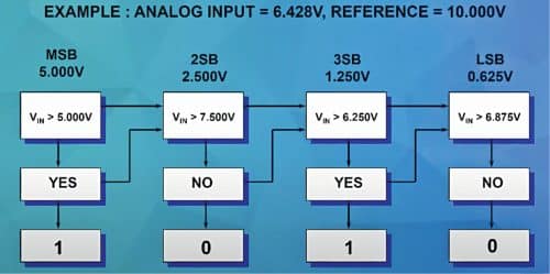
Analogue-to-digital conversion involves two steps—sampling and quantisation. Inside an ADC, a switch capacitor takes snapshots of the input signal at regular intervals (known as sampling frequency). These snapshot values are rounded off to the nearest value for digital representation.
Resolution is the first factor to consider here. It refers to the number of output bits that the ADC can generate per conversion and determines the smallest input signal that the ADC can represent.
Then comes accuracy—the close matching of the input to the desired output. Third is the sampling rate or speed, which is decided based on how fast the input signal is changing or input signal bandwidth.
A perfect reconstruction is possible only if sampling rate is equal to or greater than twice the highest frequency in the original signal. This minimum required sampling rate is known as the Nyquist rate. Though this little detail sounds harmless, it can create a major challenge between theoretical sampling and analogue-to-digital conversion. This can be avoided by band limiting the input signal to meet Nyquist rate.
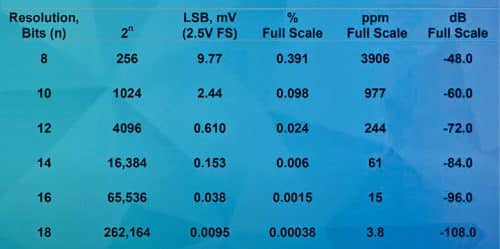
In quantisation, it is important to have a very low quantisation error; even an ideal ADC will have some minimal noise. This can be achieved by increasing the number of levels or the resolution of ADC, say, for instance, 8-bit, 10-bit, 12-bit or 24-bit.
The goal of an ADC is always to detect even a very small range of signals. So, for example, it is possible to resolve only a signal bound by the quantisation error. In lower numbers, it may be extremely difficult to detect that signal because it will all be represented by the same digital code. But when you increase the number of levels, you can detect even smaller signals.
 The ratio of the smallest resolvable signal to the largest resolvable signal is defined by the maximum achievable dynamic range. With higher resolution, you get better dynamic range and capability to even detect small signals.
For example, in a 2.5V full scale ADC, even a 95-microvolt signal can be detected with an 18-bit ADC, and a 12-bit ADC can detect only around 610 microvolts of signal. And for some analogue inputs, one must define polarity—single ended, unipolar, or differential. This should be considered if you are looking for high precision systems and want to ensure less components.
Picking the right architecture
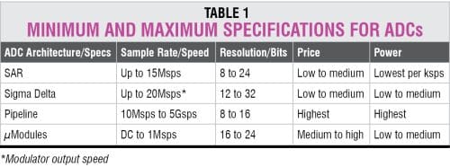
Each ADC architecture comes with its own pros and cons. Being aware of these will help you select the right type of architecture for your requirements. Some of the well-known architectures are flash, successive approximation (SAR), delta-sigma, and pipelined.
SAR ADC is the predominantly-used architecture, tailored for instrumentation, industrial control, and data type of applications. Its key features involve the ability to control conversion process, start pulse, reset logic, and comparator efficiency and other notable advantages over low power, small die area, and cost. So, this type of architecture is very well used in 8-bit, 10-bit, and 12-bit ADCs.
But the flip side is, the number of resolutions and comparisons will significantly increase conversion optimisation time. Hence, this architecture is feasible when the resolution parameter is not very high.
The other architecture is sigma delta ADC, which is used for high-precision applications requiring higher resolution. Concepts of oversampling and noise shaping, wherein the modulator frequency rate is high, the noise inline gets spread across large bandwidth. Further, noise shaping is used to shift noise out of the band of interest, which can then be removed with low pass digital filtering. Such ADCs are very popular when high resolution is desired and find application in slow-moving input signals like temperature and pressure.
Staying on top of the tech
A lot of interesting innovations are happening in this space, which could in turn do a lot of good to your application too. Integration and simplification seem to be the most effective mantras today.
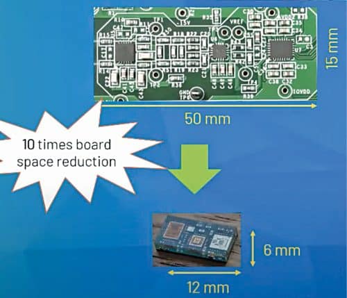
Designers are trying to integrate single-chain components like amplifiers and filters on the ADC chip itself. All discrete implementations have been moved onto a single IC, called a micro-module. This can help reduce board space significantly.
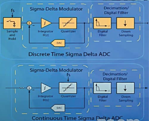
The continuous time sigma delta ADC is another new development worth watching, as this architectural approach offers major benefits of inherent anti-aliasing and resistive inputs.
In traditional signal chains there would be a requirement of high bandwidth driver to drive the switch capacitor input and low pass filter to make sure Nyquist is met and there is no aliasing. Also, there would be a reference buffer needed to drive the switched cap reference input. This adds to components and increases the bill of materials.
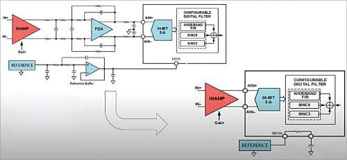
The continuous time sigma delta ADC has a resistive input and the sampling part is introduced at a much later stage, keeping the entire loop continuous. This removes the requirement of the high bandwidth driver, which is already present to solve the sample problem with it. The other benefit of this continuous loop is that any aliasing that gets introduced automatically gets rejected. Hence, the requirement of high-bandwidth driver and low-pass filter is totally removed from the signal chain, which reduces number of components, simplifies design, and makes bill of materials management simple.
It is recommended for designers to use manufacturers’ selection guides along with some basics on architecture types. The designers can use tools, devices, and design aids to support the selection process. Do not overlook input, output signals and consult data sheets or application notes, if any. As ADC technologies improve, it will lead the way for efficient electronics devices.
The article is based on a talk by Wasim Shaikh, Product Applications Manager, Analog Devices, at the Design Unconference.
Wasim Shaikh is Product Applications Manager at Analog Devices