 Doing calculations in a microcontroller based project is common. Such calculations done by the microcontroller are pre-written as a part of the code, which means that these formulae cannot be changed or altered even if a situation demands so. But what if your system has to solve equations on the fly? What if you want to define an equation to be evaluated and the microcontroller has to perform the task based on that?

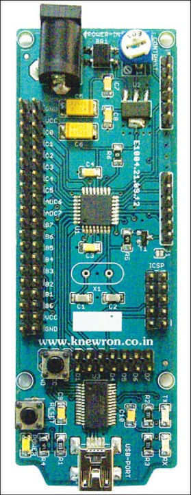
 Presented here is a handy postfix notation system that can do your calculations in practically no time, and that too without changing the source code. It can even handle parenthesis and algebraic operator precedence. Instead of explaining just the postfix notation system, algorithm and overall method, let us build a basic calculator based on this technique using Atmel’s AVR microcontroller. Fig. 1 shows the author’s prototype.
Circuit and working
Fig. 2 shows the circuit diagram of a calculator using postfix notation. The circuit is built around microcontroller ATmegA168 (IC1), USB-to-UART converter FT232RL (IC2), 16×2 LCD display (LCD1) and a few easily-available components. You can also use ATmeg168 Development Stick, which is available with EFY associates Kits‘n’Spares.

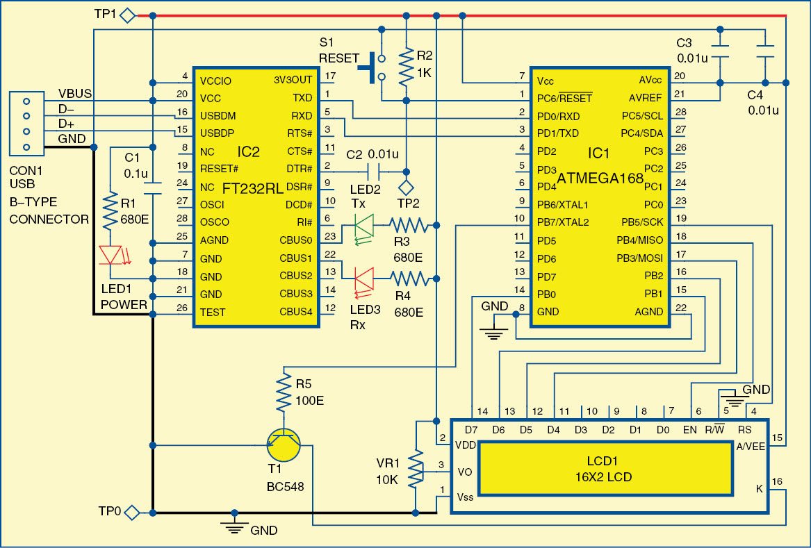
The circuit is powered directly through USB port, which provides 5V supply for the circuit to operate. LED1 indicates presence of power in the circuit. Pins 15 and 16 of IC2 are connected to D+ and D- of USB port and pins 1 and 5 of IC2 are connected to RXD and TXD pins of microcontroller IC1, respectively.

LCD1 is used to display the calculated result. Port pins PB3 through PB0 of IC1 are connected to data pins D4 through D7, and port pins PB4 and PB5 are used to provide control signals EN and RS to LCD1, respectively. R/W pin is grounded permanently, as shown in Fig. 2. Switch S1 is used to manually reset microcontroller IC1.
Postfix notation
The postfix notation method was introduced in 1954 and was first used in desktop calculators by HP in 1963. However, now almost all the calculators deploy it to perform calculation of user inputs. In postfix notation the operators follow their operands; for instance, to add 4 and 6, one would write 4 6 + rather than 4 + 6. If there are multiple operations, the operator is given immediately after its second operand. So the expression ‘1 − 4 + 6’ written in conventional notation would be written as ‘1 4 − 6 +’ in postfix. That means, first subtract 4 from 1 and then add 6 to that.
An advantage of postfix is that it obviates the need for parentheses, which are required by normal notations, and thus removes ambiguity from the formulae. For instance, 1 − 4 ×6 can also be written 1 − (4×6) and it is quite different from (1 − 4)×6. In postfix, the former could be written as 1 4 6 × −, which unambiguously means 1 (4 6 ×) −, whereas the latter could be written 1 4 – 6 × or 6 1 4 – ×. As the notation result is always context-free, once an equation is converted to postfix notation, it becomes easier for a computer to evaluate the same using outside-in evaluation sequence.
Working of the circuit is simple. Once the program is running, the input equation to be solved can be provided using hyper-terminal or other similar software like X-CTU. The equation and the calculated result will be displayed on the LCD. (Refer construction and testing section for details.)
Software
 The program code is written in ‘C’ language and compiled using AVR Studio 6.0. The hex file is burnt into the microcontroller using a suitable programmer.
Postfix algorithm
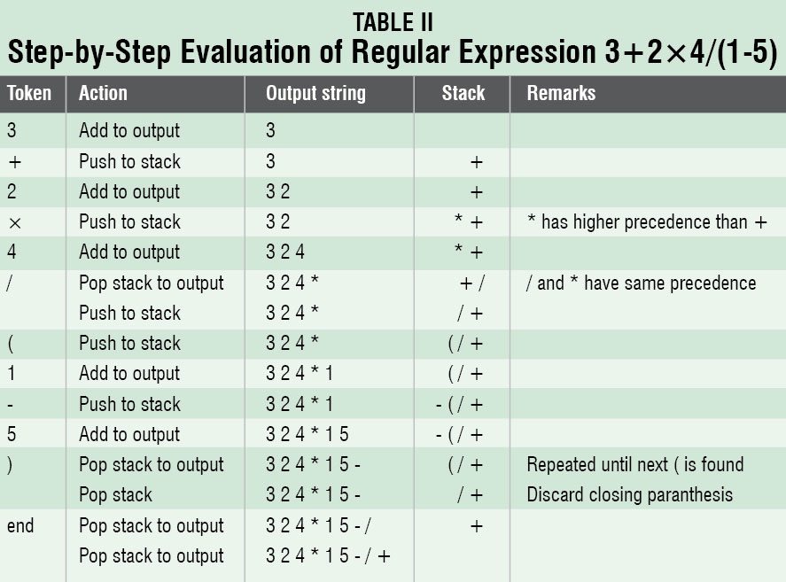
The method is stack-and-queue dependant and uses a stack for storing functions (aka operators) and a simple queue to hold numbers (aka operands). Due to the nature of operations performed in this algorithm, it is also called a ‘shunting yard algorithm’ since the operation resembles a railroad shunting-yard methodology. Table II shows step-by-step evaluation of a regular expression using postfix algorithm.
Once parsing is done, rest of the part is much easier to perform. For evaluating the answer following steps have been performed in the source code:
1. Initialise an empty stack
2. Scan the postfix notation string from left to right
3. If the token read is operand, push it into stack
4. Else, if the token read is operator (that would mean that there are at least two operands already present in the stack):
(i) Pop these two operands from stack
(ii) Perform the operation as per the operator
(iii) Push the results back into the stack
5. Once the string scanning is complete, there would be only one element present in the stack, which is the final answer.
Construction and testing
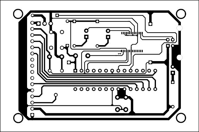
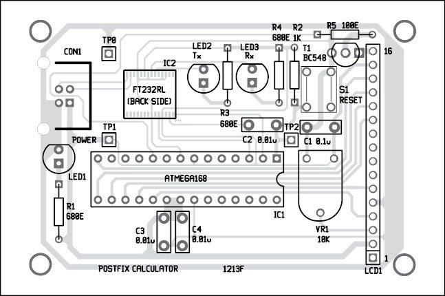
A single side PCB layout for the postfix calculator circuit is shown in Fig. 4 and its component layout in Fig. 5. Assemble the circuit on the recommended PCB to save time and minimise assembly errors. Use an IC base for microcontroller IC1. IC2 being an SMD package it should be mounted on the solder side.
Once the PCB is ready, follow the steps below to get the project running:
1. Install the FTDI drivers on your computer from the FTDI website corresponding to your operating system.
2. Connect the PCB to the computer through the provided USB interface, and you should see USB-to-serial converter detected in the device manager.
3. The microcontroller should already be programmed. Now press the reset button and the LCD will show ‘my calci’ as in Fig. 1.
4. Open hyper-terminal or a similar program and select the right COM port.
5. Write the equation to be calculated in the hyper-terminal window and write ‘=’ at the end.
Download PCB and Component Layout PDFs: click here
Download Source Code: cllck here
On completion of the last step, the equation and the calculated result appear on the window as well as the LCD.
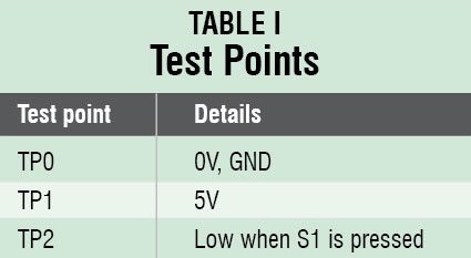
To test the circuit for proper functioning, check 5V supply at TP1 with respect to TP0. The presence of supply is also indicated by LED1. The reset to the system can be observed at TP2. LED2 and LED3 indicate to and fro data communication between IC2 and IC1. Ensure that correct baud rate is selected (19200 bps as mentioned in the source code) for communication between MCU and PC.