


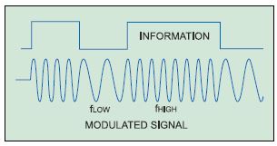
Frequency shift keying (FSK) is a frequency modulation scheme in which digital information is transmitted through discrete frequency changes of a carrier wave. It uses a pair of discrete frequencies to transmit binary (0s and 1s) information. Information and modulated signals are shown in Fig. 1.
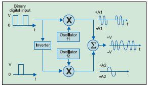
A typical block diagram of an FSK transmitter is shown in Fig. 2. Binary data is modulated with high-frequency sinusoidal signal (f1) and inverted binary data modulated with low-frequency sinusoidal signal (f2). Outputs are combined using an adder circuit to provide the frequency shift keyed signal, which can be transmitted via telephone lines, fibre optics or wireless media. Block diagram of the FSK receiver is shown in Fig. 3.
The transmitter circuit is built around CD4066B quad-bilateral switch (IC1), a digital pulse generator (XFG3), high-frequency oscillator (XFG1), low-frequency oscillator (XFG2) and 7404 hex inverter (IC2). Details of the source, frequency and nature of signals are given in the table.

| Specification of Signals | ||
| Source | Nature of signal | Specification |
| XFG1/f1 | Sinusoidal wave as carrier I | 50kHz, 10V pk-pk |
| XFG2/f2 | Sinusoidal wave as carrier II | 9kHz, 10V pk-pk |
| XFG3 | Square wave as data signal | 500Hz, 10V pk-pk |
A high-frequency sinusoidal signal from XFG1 is applied at pins 1 and 8 of IC1, which is controlled by binary data from XFG3 at pins 13 and 6 of IC1. A low-frequency signal from XFG2 is applied at pins 4 and 11 of IC1, which is controlled by binary inverted data applied at pins 5 and12 of IC1.
The quad-bilateral switch (IC1) produces two amplitude shift keyed signals at pins 2 and 3, which are combined to get the frequency shift keyed signal in XSC1. We are using the remaining two switches for FSK signal generation for the demodulator circuit to ignore the feedback problem.
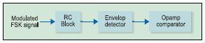
The receiver circuit is built around high-pass filters (R5 and C2), envelope detectors (D1, C1 and R1) and op-amp comparator circuits (R2, R3, D2, D3 and IC3).
In this section our objective is to generate binary data information (modulating signal). So, initially, we are required to block-frequency components using high-pass filters having a cut-off frequency f =1/ (2×3.14×C2×R5), which is approximately 10kHz. This blocks the 9kHz low-frequency signal.
After elimination of low frequency, output of HPF is fed to the envelope detector. The envelope detector, a combination of half-wave rectifier with diode 1N4007 and parallel combination (LPF) of resistance (R1) and capacitor (C1), provides the envelope of rectified signal that passes through the operational amplifier working as comparator to generate the square wave using a threshold of 6V. This way we get a demodulated signal with small delay.
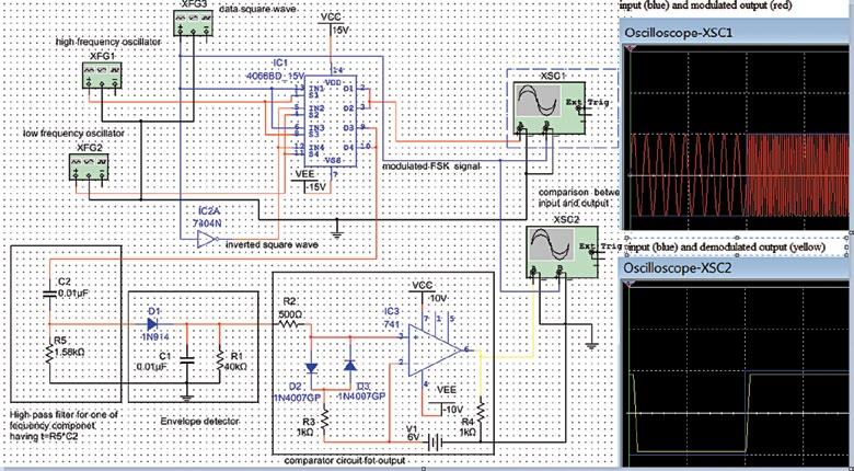
The schematic, modulating signal and results of modulated and demodulated signals are shown in Fig. 4. The circuit has been simulated in NI Multisim software.
Download source code: click here
CD4066B quad-bilateral switch (IC1) sir this ic is not availabule in my multisim software
can you please help me sir