
 Event log data is a unique source of information for security, audit, compliance and troubleshooting purposes. An event logger enables you to view the log of a series of events. This can be done not only at the time of occurrence of the events but also any time later. The event logger provides an accurate time and date at which a particular event has occurred, which is essential for many applications.
In this event logger article, we also demonstrate the use of a DS1307 real-time clock (RTC) chip, switches and an LCD module. The RTC chip provides time components of hours, minutes and seconds in addition to the year, month and day.
In this project, pressing a switch is regarded as an event. When the event occurs, it is recorded in memory locations of the microcontroller. This information from the microcontroller can be retrieved and seen on the LCD module and HyperTerminal.

Circuit and working of Event Logger
Fig. 1 shows the circuit of RTC-based event logger. It comprises regulator 7805 (IC1), microcontroller P89V51RD2 (IC2), RS232 interface MAX232 (IC4), RTC chip DS1307 (IC3), LCD module and a few discrete components.
Microcontroller. The P89V51RD2 is an 8-bit 80C51 microcontroller with 64kB Flash and 1024 bytes of data RAM. It has three 16-bit timers/counters, programmable watchdog timer, eight interrupt sources with four priority levels, serial peripheral interface (SPI) and enhanced UART, programmable counter array with PWM and capture/compare functions, and four 8-bit input/output (I/O) ports. It also has an on-chip oscillator and clock circuitry, which is operated at up to 40MHz crystal. It supports 12 clocks per machine cycle (default) and 6 clocks per machine cycle modes, which can be selected via software. The Flash program memory supports both parallel programming and serial programming.

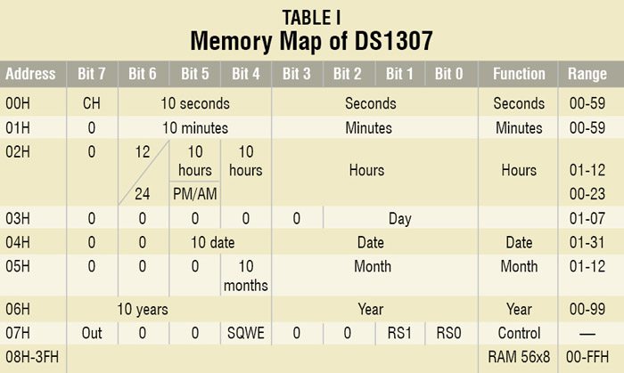
 Real-time clock chip. DS1307 is a serial RTC chip with calendar function. This chip also incorporates 56 bytes of non-volatile RAM. Data and address are transferred serially through I2C bi-directional bus, which obviates the need for a large number of interface lines. In this chip, the clock operates in either 24-hour or 12-hour format with AM/PM indicator. In calendar mode, end of the month is automatically adjusted for months with less than 31 days and leap year compensation. The memory map of DS1307 is shown in Table I.
Clock pulse to the RTC is provided by a 32.678kHz crystal. As per convention of I2C interface communication, device address while writing into the RTC chip is 0xD0 and device address while reading data from the RTC chip is 0xD1.
Using SCL and SDA lines, the microcontroller can read/write data from/to the memory of the RTC chip.
Some of the conditions to communicate through the I2C bus are:
Clock and data transition. The SDA line is normally pulled high with an external device. Data on the SDA line can change only when SCL line is low. Data changes during a high SCL line will indicate a start or stop condition.
Start and stop. The start condition is a high-to-low transition of SDA line while SCL line is high. The stop condition is a low-to-high transition of SDA line while SCL line is high.

Acknowledge. All addresses and data words are serially transmitted to and from the RTC chip in 8-bit words. The RTC sends a zero to acknowledge that it has received each word. This happens during the ninth clock cycle.
For example, to set the time ‘8:32:59’ into the RTC, the following interface protocol is followed:
1. Start bit is sent from microcontroller IC2 (master) to RTC IC3 (slave).
2. Then 0xD0 is sent to the slave. This is the address of the RTC (as mentioned in its datasheet). Also, the least significant bit (LSB) of 0xD0 is zero, which means it is a writing command for the slave. The slave sends an acknowledgement (ACK) after receiving this byte.
3. 0x00 is sent to the slave. It is the starting address in the RTC on which we want to write the first byte. The slave sends an ACK after receiving this address byte.
4. 0x59 (value of seconds) is sent to the slave. This is the value we want to save in the RTC on 0x00 address. The slave sends an ACK after receiving this byte.
5. 0x32 (value of minutes) is sent to the slave. This is the value we want to save in the RTC on 0x01 address. The slave sends an ACK after receiving this byte.
6. 0x08 (‘8’ is the value of hours, while ‘0’ means 24-hour time format) is sent to the slave. This is the value we want to save in the RTC on 0x02 address. The slave sends an ACK after receiving this byte.
7. A stop bit is sent to the slave.
8. After receiving this command, slave DS1307 sets its time to 8:32:59.
To read back the data from the RTC using the microcontroller, the interface protocol is:
1. Start bit is sent from microcontroller IC2 (master) to RTC IC3 (slave).
2. 0xD0 is sent to the slave. This is the address of the RTC. The slave sends an ACK after receiving this byte.
3. 0x00 is sent to the slave, setting the address pointer to 00. The slave sends an ACK after receiving this address byte.
4. 0xD1 is sent to the slave. This is the address of the RTC (as mentioned in its datasheet). Also, the LSB of 0xD1 is ‘1,’ which means it is a reading command for the slave. The slave sends an ACK after receiving this byte.
5. The data (like seconds, minutes and hours) is read from slave address location.
6. Finally, a stop bit is sent to the slave.
7. After this command, time, say, 8:33:10, is read and can be displayed on the LCD module.
The procedure is similar for day, month and year too.
To derive the power supply for the circuit, the 230V AC mains is stepped down by transformer X1 to deliver a secondary output of 9V, 500 mA. The transformer output is rectified by a full-wave rectifier comprising diodes D1 through D4, filtered by capacitor C1 and regulated by IC1. Capacitor C2 bypasses the ripples present in the regulated supply. LED1 acts as the power indicator and R1 limits the current through LED1. Rechargeable battery BATT.2 is used for power backup. Battery is charged through resistor R8 and diode D5. Resistor R8 limits the charging current. Diode D6 protects the battery from discharging when mains is present.
Data pins D0 through D7 of the LCD are connected to port pins P2.0 through P2.7 of microcontroller IC2, respectively. Control pins register-select (RS), read/write (R/W) and enable (E) are connected to port pins P3.5, P3.6 and P3.7, respectively. Preset VR1 is connected to pin 3 of the LCD for contrast control. Power-‘on’ reset is provided by the combination of resistor R2 and capacitor C3. Switch S20 is used for manual reset. An 11.0592MHz crystal along with two 33pF capacitors provides the basic clock frequency to microcontroller IC2.


Download PCB and component layout PDFs: click here
Download source code: click here
A 16-key numeric keypad for time/date entry is connected to port P0 of IC2. To economise on the use of I/O pins, we have used only eight pins for scanning and sensing sixteen keys. The keypad is arranged in a 4×4 matrix. There are four scan lines/pins, which are set in output mode, and four sense keys, which are used as input lines. Switches S17 through S19 are connected to port pins P1.3 through P1.5 of the microcontroller for event logging, display on the LCD and sending to PC’s HyperTerminal, respectively.
Port pins P1.0 and P1.1 of the microcontroller are connected to SDA and SCL lines of IC3, respectively. The microcontroller can write the data to and read from the RTC through SCL and SDA lines. RS232 interface is used to display the data on the PC’s HyperTerminal using USART transmission.
Working of the circuit is simple. When you power-‘on’ the system, you will see messages ‘Welcome’ and ‘EFY Time Logger’ displayed on the first and second lines of the LCD, respectively. After an interval of a second, messages ‘Set Clock’ and ‘Enter Hour’ are displayed on the first and second lines of the LCD, respectively. Enter hours using the numeric keypad. Then it will ask you to enter minutes, seconds, date, month and year one by one. The time and date are displayed on the first and second lines of the LCD after all the entries are done. Pressing of switch S17 is an event, which is stored with date and time in the logs. Last ten logs can be seen on the LCD by pressing switch S18. Last 100 entries can be retrieved using HyperTerminal. Connect the serial port and set up the HyperTerminal. Now if you press S19, the last 100 entries will appear on the HyperTerminal.
Construction and testing
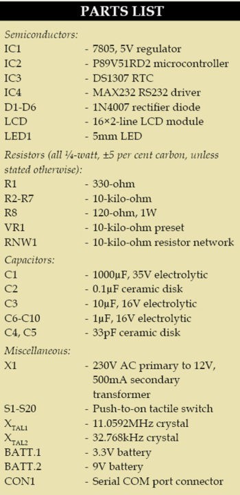
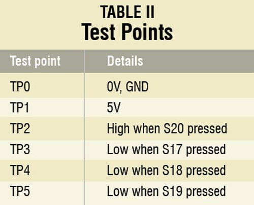
An actual-size, single-side PCB for the circuit of the event logger (Fig. 1) is shown in Fig. 2 and its component layout in Fig. 3. Assemble the circuit on a PCB as it saves time and minimises assembly errors. Carefully assemble the components and double-check for any overlooked error. Use IC bases for the microcontroller and the RTC. Before inserting the ICs, check the supply voltage. Using preset VR1 set the LCD contrast for proper display. To test the circuit for proper working, check the voltages at different points as per Table II.
Software
The source program for the microcontrollers is written in ‘C’ language and compiled using Keil µVision4 compiler. The generated hex code is burnt into the microcontroller by using a suitable programmer. The program is well-commented and easy to understand.
On reset/power-‘on,’ the microcontroller executes the main program. It first initialises variables, baud rate and the LCD, then starts displaying the messages for setting the time and date using start( ) function. Time and date are to be entered from the numeric keypad. Key_scan( ) function scans for key entries. Message ‘Invalid Key’ is displayed on the LCD if any wrong key is pressed. A continuous loop always displays the date and time and checks the status of switches S17 through S19. Function DS1307_get(unsigned char addr) is used to read the time and date, which are displayed on the LCD by function sendlcd(unsigned char value).
When an event occurs (switch S17 pressed), the time and date of the event are saved on the microcontroller’s memory location by data_shift( ) function and message “You are logged” is displayed on the LCD. Switches S18 and S19 are used to display the last ten recorded data on the LCD one by one and the last 100 recorded data on the HyperTerminal. Functions DS1307_settime(unsigned char hh, unsigned char min, unsigned char ss) and DS1307_setdate(unsigned char dd, unsigned char mm, unsigned char yy) are used to set the time and date, respectively.