 This article shows you how to create a DIY laser light security alarm, perfect for enhancing home security. The best part?
It’s a simple project anyone can build to help protect their home from theft.
TOOLS REQUIRED
- Soldering iron
- Soldering flux
- Solder wire
- Small hand drill machine
Components Required
- Plain PCB (printed circuit board)
- Scrubber
- PCB etching
- Double-sided tape
- Resistor 100 Ω – 03nos.
- LDR (light dependant resistor)-01no.
- LED (light emitted diode)-01no.
- Transistor (BL548) -02 nos.
- Buzzer
- Switch
- DC socket (Nokia cellphone small charging pin)
- Adapter -5volt (nokia charger)
- Battery holder
- Battery
- Laser light
- Switch
Construction & Testing for Laser Light Security Alarm
Step 1
Tracing the circuit
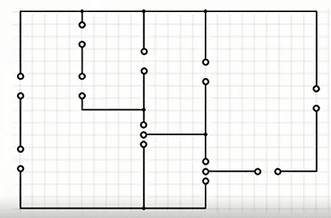
Take a permanent marker and make a rough layout or path draw on your PCB as shown in figure 1.


Step 2
Clean the PCB with the help of a scrubber and after taking a small size container and some PCB etching solution (Ferrous Chloride), prepare a solution of etching by mixing the ferrous chloride and water in a container. Dip PCB into solution and shake it for 10 minutes, now take out the PCB and wash it thoroughly.
Step 3
Drill few holes on PCB with the help of small hand drill for mounting other electronic components.
Find the location of electronic components from layout and placing them carefully on their respective positions.
Solder the electronic components on PCB and assemble the laser light and solder it carefully with the battery holder and also solder a switch to positive terminal of battery holder.
Step 4
Final step
Carefully placed the battery holder and after checking the output voltage of circuit with a multimeter.
After checking the circuits again for proper placement, press the switch ‘ON’.
Now, when you put your finger in front of laser, you will find that the buzzer would turn on thus producing an alarm. When you ‘OFF’ the switch the buzzer will not make any sound.
Your Security System is ready.
Customization Ideas:
- Laser Path Redirection:
- Use small mirrors to reflect the laser beam across multiple directions, creating a web-like barrier to cover a larger area or multiple entry points like windows and doors.
- Adjustable Sensitivity:
- Incorporate a potentiometer to control the sensitivity of the LDR, allowing it to work in varying light conditions (e.g., bright sunlight or dim indoor lighting).
- Multiple Alarm Types:
- Add more outputs like flashing LEDs or a vibrating motor to create different alarm types that trigger when the laser is interrupted.
Project Applications:
- Home Security:
- Use the system near doors or windows to detect intrusions and protect your home from theft or unauthorized entry.
- Garage or Shed Security:
- Install the laser alarm in garages or outdoor sheds to safeguard vehicles, tools, or equipment.
- Perimeter Monitoring:
- Set up the alarm around the perimeter of your property or garden to detect when someone crosses into your space.
- Office or Personal Workspace Security:
- Place the system at the entrance of an office or workspace to alert you when someone enters, protecting personal or valuable items.
- Temporary Event Security:
- Use the laser alarm in event spaces or exhibits to guard restricted areas or valuables, adding extra security without installing complex systems.
Shri Himadree Bhusan Sahoo is an Electrical Engineering student and Electronics Enthusiasts
This article was first published on 13 April 2018, and updated on recently 23 October 2024


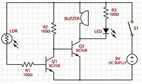
in Schematics the transistors Q1 & Q2 are shown BC458 instead of BC548
The transistor Q1& Q2 is a BC548
NPN transistor.
Thanks
Himadree
system testing , input & output design send me bro
That article is small but curious to young generation.
Please change Transistor (BL548) to BC548
can you explain working of this circuit?
Sir this circuit is very interesting. Can u send me the PCB layout in pdf form and plz explain the working of this circuit. I will be very thankful to you.
Hi, this project is not verified by EFY labs. This is an untested circuit so we don’t have PCB and component layout for this particular circuit.