A new method bonds 2D semiconductor layers without glue. This could make devices smaller and faster. Read on!
Electronics engineers aim to make devices smaller while improving their speed, performance, and efficiency. Two-dimensional 2D semiconductors, ultra-thin single-layer materials with controllable electrical properties, show promise for this goal. Compared with conventional semiconductors, these thin materials could enable smaller devices without sacrificing performance. However, producing high-quality 2D semiconductor wafers and stacking them precisely has been difficult.

Researchers at Songshan Lake Material Laboratory, the Chinese Academy of Sciences, and other institutes have now developed a method to directly bond two 2D semiconductor wafers without using additional materials. Their approach, reported in Nature Electronics, could advance the creation of high-performance transistors and other electronic components based on 2D semiconductors.
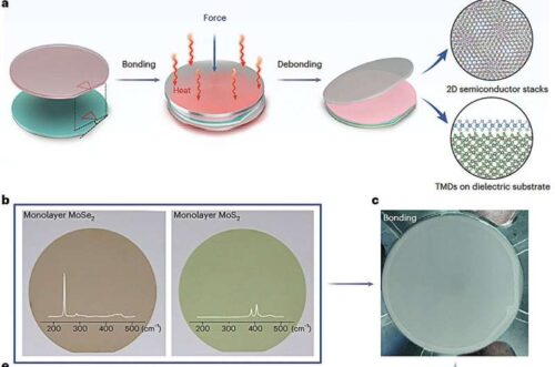
Two-dimensional (2D) semiconductors are emerging as promising building blocks for advanced electronic devices. However, fabricating high-quality 2D semiconductor wafers with engineered layers remains challenging. A new method has been developed that uses direct wafer bonding and debonding for semiconductor monolayers grown epitaxially on high-adhesion substrates such as sapphire.
Traditionally, bonding 2D semiconducting materials to create slightly thicker structures with desired properties has relied on glue-like intermediate materials. While effective, these materials can contaminate the interface between the two layers.

The new bonding strategy produces very flat, clean, and chemically active 2D semiconducting layers that adhere to each other without intermediate materials. The process works in both vacuum and glovebox environments and enables wafer-scale uniformity, precise control over the number of layers, and accurate tuning of the interlayer twist angle.
Using this method, various structures composed of 2D monolayers have been successfully fabricated. These structures feature different numbers of layers and twist angles. The approach can create both homostructures and heterostructures, including combinations of molybdenum disulfide (MoS₂) and molybdenum diselenide (MoSe₂). It also allows direct bonding of monolayer MoS₂ onto high-κ dielectric substrates such as HfO₂ and Al₂O₃ while preserving the material’s intrinsic electronic properties.
This reversible bonding strategy could enable the engineering of smaller, faster, and higher-performing electronic devices. In the future, it may be used to create a wide range of carefully engineered structures integrating multiple 2D semiconductor monolayers.