


Researchers have developed an AI-driven semiconductor analysis technique that extracts critical material properties from simple transistor measurements in less than a millisecond, potentially transforming chip development and manufacturing.
Artificial intelligence is showing a new way to accelerate semiconductor characterization, enabling engineers to uncover hidden material properties from routine transistor measurements almost instantly. Researchers from the Institute of Science Tokyo have developed a machine-learning framework that can infer key semiconductor parameters in under one millisecond, a task that traditionally requires extensive simulations and can take hours or even days.

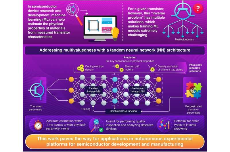
The breakthrough addresses a long-standing challenge in semiconductor engineering known as the inverse problem. While measuring the electrical behavior of a transistor is relatively straightforward, determining the underlying material characteristics responsible for that behavior is far more complex. Multiple combinations of physical parameters can produce nearly identical electrical responses, making it difficult to identify the exact properties of a semiconductor device.
To overcome this obstacle, the research team designed a tandem neural network architecture. The first neural network estimates material properties from measured transistor data, while a second pretrained network reconstructs transistor behavior from those estimated properties. By linking the two models, the system learns to generate solutions that are both physically meaningful and mathematically consistent, significantly improving prediction accuracy.
The AI model was trained using 1,000 datasets from amorphous indium-gallium-zinc oxide (a-IGZO) transistors. It analyzed six critical semiconductor parameters, including defect densities, trap-state characteristics and electron mobility. Despite handling parameter ranges roughly 1,000 times wider than those used in previous machine-learning studies, the system achieved near-perfect prediction accuracy from a single current-voltage measurement.
Researchers also validated the approach on real laboratory-fabricated transistors operating under different conditions. The model successfully reproduced measured device behavior without requiring additional optimization steps, demonstrating its practical applicability. According to the team, the AI approach delivers a speed improvement exceeding six orders of magnitude compared with conventional simulation-based characterization techniques.
The technology could have significant implications for semiconductor manufacturing, enabling rapid quality inspection of devices directly on production lines. It may also support autonomous research laboratories where AI systems design, execute and analyze experiments with minimal human intervention. Beyond semiconductors, the framework could be adapted to solve complex inverse-analysis problems in materials science, chemistry and photonics, opening new opportunities for AI-assisted scientific discovery.
