


Researchers have developed a single-atom-thick coating that could solve a major semiconductor interconnect challenge, enabling smaller, faster and more reliable chips while preserving valuable space for copper wiring.
A breakthrough in semiconductor materials engineering may help the chip industry overcome one of the biggest obstacles to continued miniaturization. Researchers have demonstrated an atomically thin coating that can replace conventional copper barrier and liner layers used inside integrated circuits, potentially improving performance while freeing up critical space in next-generation chip designs.

As transistors continue to shrink, the metal interconnects that carry signals across a chip are becoming increasingly difficult to scale. Modern copper wiring relies on barrier and liner materials that prevent copper atoms from diffusing into surrounding structures while maintaining electrical reliability. However, these protective layers consume a growing share of the available wiring space as dimensions shrink.
The research team developed a coating based on tungsten disulfide (WS₂), a two-dimensional material only 0.7 nanometers thick. Despite its atomic-scale thickness, the material successfully performed the functions typically handled by a much thicker barrier-liner stack measuring around 6 nanometers. Testing showed the WS₂ layer delivered roughly five times better performance while occupying nearly one-tenth of the thickness of conventional solutions.
The space savings become particularly important in future semiconductor nodes. In a projected 20-nanometer-wide copper wire, traditional barrier materials could consume approximately 40% of the wire’s diameter. The atom-thin WS₂ coating would require only about 7%, leaving significantly more room for copper to carry electrical current. This could help maintain conductivity and reduce resistance as chipmakers push toward denser designs.
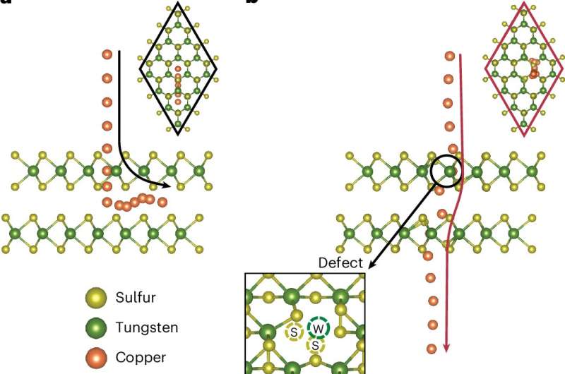
Researchers also evaluated the material’s ability to block copper migration, a critical requirement for long-term chip reliability. Under thermal stress, unprotected copper reacted with underlying silicon and formed defects. Devices protected by the WS₂ layer showed no such reaction. Electrical stress testing further indicated that the coating extended projected wire lifetimes by more than ten times compared with unprotected structures.
Computational analysis revealed that the material’s polycrystalline structure plays a key role in its effectiveness. Randomly oriented grains create a complex pathway that makes it difficult for copper atoms to penetrate the barrier, enhancing protection without increasing thickness.
The development could provide semiconductor manufacturers with a new route to continue interconnect scaling at advanced process nodes, addressing a growing bottleneck that threatens future gains in chip performance and energy efficiency.
