

A new two-dimensional semiconductor material could address a major limitation in next-generation chip design, enabling smaller transistors, improved switching performance, and potentially lower-power electronics.
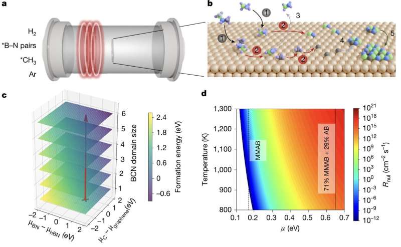
An atomically thin semiconductor made from boron, carbon, and nitrogen could help overcome a key challenge in developing smaller, more energy-efficient transistors. The material, boron carbon nitride (BCN), demonstrates promising performance as a p-type semiconductor, potentially enabling future chips with densely packed transistors and reduced power consumption.
Researchers led by Vincent Tung at the University of Tokyo developed wafer-scale BCN films that support efficient hole transport while maintaining stable electrical switching. The findings, published in Nature, address a long-standing limitation in two-dimensional semiconductor technology: achieving reliable p-type transistors that perform alongside their n-type counterparts.
Modern chips use both transistor types to process electrical signals. While n-type transistors conduct through electrons, p-type transistors rely on positively behaving charge carriers called holes. Although several atomically thin materials have demonstrated promising electron transport, developing equally effective p-type materials has remained difficult.
Carbon Doping Enables Hole Transport
To develop the material, the researchers introduced carbon atoms into boron nitride, an atomically thin insulating material with a honeycomb-like atomic structure. Carbon replaced some nitrogen atoms, creating holes that could carry electrical charge.
The team used a vapour-based epitaxial growth process to distribute carbon throughout the material while preserving its underlying structure. By carefully controlling the supply of boron, nitrogen, and carbon, the researchers prevented excessive carbon clustering and produced wafer-sized BCN films, including on patterned silicon chips.
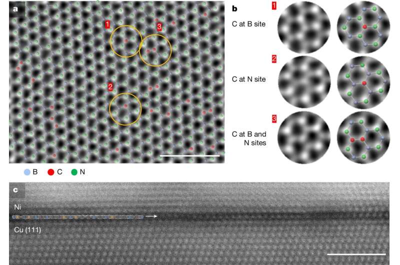
Atomic-resolution microscopy confirmed the material’s structure and the distribution of carbon atoms. The researchers subsequently fabricated and tested 224 transistors under ambient conditions.
The devices demonstrated an on-to-off current ratio of approximately 100 million to one. This indicates that the transistors could conduct strongly when switched on while suppressing current when switched off. The material also remained stable in air, addressing an important practical requirement for semiconductor manufacturing.
Potential for Compact, Low-Power Chips
The results could support future semiconductor architectures that combine atomically thin n-type and p-type transistors. Such devices could potentially be stacked vertically, increasing transistor density without requiring a proportional increase in chip footprint.
However, further engineering is required before commercial deployment. The researchers need to optimise metal contacts to improve electrical connections and reduce associated performance losses. They must also reduce the transistor dimensions and lower the material’s growth temperature, currently around 1,000°C, which could damage existing components during chip fabrication. If these challenges are resolved, BCN could contribute to future high-density, low-power computing hardware and advanced semiconductor integration.