


This atom-thin coating tackles a critical interconnect bottleneck, offering chipmakers a practical route to next-generation semiconductor design.
Researchers from National University of Singapore (NUS) and Applied Materials have developed an ultra-thin tungsten disulfide(WS2) coating that could help overcome a major challenge in semiconductor scaling. The atom-thick material combines the functions of conventional barrier and liner layers used in copper interconnects, potentially enabling smaller, faster, and more reliable chips.

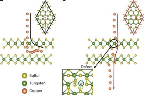
Copper interconnects are the microscopic wiring networks that carry signals between billions of transistors inside modern processors. As semiconductor devices continue to shrink, the protective layers surrounding these copper lines occupy a growing portion of the available space, increasing electrical resistance and making further miniaturisation more difficult.
To address this issue, the research team developed a single-layer WS2, coating measuring just 0.7nm thick. Unlike conventional solutions that rely on multiple protective layers, the new material performs both barrier and linear functions in a single layer, freeing up more space for copper within the interconnect structure.
According to the researchers, the coating promotes smoother copper deposition while preventing copper atoms from migrating into surrounding materials. Such migration is a common cause of performance degradation and reliability issues in advanced semiconductor devices. Tests also showed improved conductivity and enhanced durability compared with unprotected structures

Another significant advantage is its compatibility with existing semiconductor manufacturing processes. The researchers demonstrated a low-temperature deposition technique that can be integrated into current fabrication lines, potentially simplifying the transition from laboratory research to commercial production.
The development comes at a time when the semiconductor industry is increasingly looking beyond traditional transistor scaling to maintain performance gains. Interconnect technologies are emerging as a critical area of innovation, and solutions that reduce resistance while preserving reliability are attracting growing attention.
By reducing the space required for protective layers without compromising the performance , the atom-thin WS2 coating could support future generations of high-performance and energy- efficient processors. The work also highlights the growing importance of advanced materials in overcoming physical limitations and extending the roadmap for next-generation semiconductor technologies.
