




Could a material already used in electronics also unlock better energy storage and memory? Researchers have confirmed hafnium oxide has an unusual electrical property.
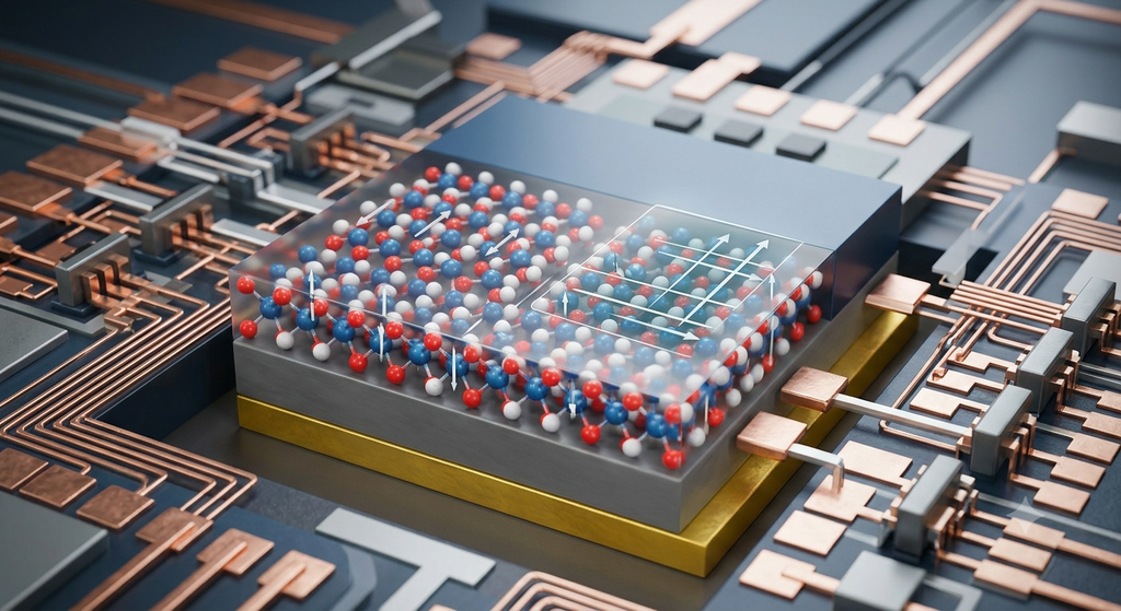
University of Nebraska–Lincoln researchers have demonstrated that hafnium oxide, or hafnia, is inherently antiferroelectric, resolving a long-standing debate over the material’s electrical behaviour and strengthening its potential for advanced electronic applications.
Antiferroelectric materials can switch between electrically neutral and polarised states when voltage is applied. This behaviour allows them to store and release energy, making the material class relevant to compact capacitors, memory technologies and solid-state cooling. Hafnia is particularly significant because it is already compatible with modern electronics and does not rely on lead, which is present in many other antiferroelectric materials.
The researchers showed that hafnia’s behaviour is intrinsic rather than an artificial effect caused by trapped or redistributed electrical charges. This distinction matters because it establishes the material as a genuine member of the antiferroelectric class and could make it a useful platform for further device research.
The team also found that the property remains stable as the material becomes extremely thin. Using pulsed laser deposition, they produced a hafnium oxide layer on a crystal substrate that stabilised the required atomic arrangement. Antiferroelectric behaviour persisted down to a thickness of 0.6 nanometres and remained stable at temperatures reaching 850°C.
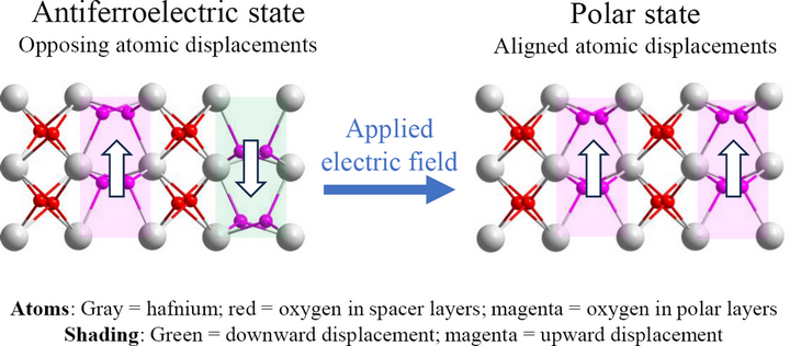
Electrical measurements confirmed the characteristic behaviour associated with antiferroelectricity, including a distinctive double-hysteresis loop, opposing electric dipoles and boundaries between regions with different polarisation states. Theoretical modelling and atomic-scale imaging provided additional support for the experimental results.
The findings could eventually support smaller high-performance capacitors, energy-efficient memory and compact solid-state cooling technologies. Because hafnia is already widely used in electronics, its compatibility with established manufacturing approaches could also make it easier to investigate than entirely unfamiliar materials.
“This is a turning point,” says Alexei Gruverman, Charles Mach University Professor of physics at the University of Nebraska–Lincoln. “Now, we can categorise hafnia as a true antiferroelectric.”


