


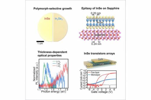
Researchers at the University of Pennsylvania School of Engineering and Applied Science have developed a high-efficiency 2D semiconductor on a full-scale, industrial-grade wafer. In which indium selenide (InSe), can be applied at temperatures sufficiently low to allow integration with a silicon chip.
The semiconductor sector continuously evolves, focusing on enhancing computing power, reducing chip sizes, and efficiently managing power in densely packed circuits. Meeting these needs calls for innovations surpassing conventional silicon-based approaches to accommodate the growing demands of computing applications. There is a pressing need for creative changes in chip materials and designs to support the expanding roles of computing devices, particularly considering the inherent 3D limitations of silicon that restrict its reduction to finer scales.

The University of Pennsylvania School of Engineering and Applied Science has succeeded in cultivating a 2D semiconductor that aligns with industrial-scale wafer dimensions. This has been facilitated using indium selenide (InSe), which permits deposition at temperatures conducive to maintaining the integrity of the silicon base.
The limitations have shifted the focus towards two-dimensional (2D) semiconductors, characterised by an almost non-existent height, offering a promising pathway for industry specialists, researchers, and microelectronics manufacturers. The advent of thinner chip constituents heightened regulation and accuracy in electrical flow within devices, coupled with reduced energy consumption. Integrating a 2D semiconductor atop its silicon counterpart could minimise chip surface area encapsulated within a delicate film. Only recently, the attempts to actualise this concept met with failures due to an array of challenges encompassing high-temperature requirements for deposition, which inadvertently compromised the silicon base, and inadequate electronic properties, including energy consumption rates, speed, and precision. Achieving the necessary purity levels at industry-compliant scales remained elusive.
Leveraging the vertical metal-organic chemical vapour deposition (MOCVD) technique surmounted the challenges of achieving a balanced 50:50 chemical structure across a substantial area. This approach pivoted on sequentially introducing indium and selenium, thereby preventing unwanted chemical structures and ensuring a uniform elemental ratio across the entire wafer. The team aligns the crystal directions within the material, fostering a conducive environment for electron transport, further augmenting the semiconductor’s quality. This accomplishment marks meeting critical industry and material standards, thereby poised to revolutionise semiconductor manufacturing by ushering in an era of optimised purity, scalability, and performance in advanced computing technology.