




How a room temperature chip patterning process is enabling simpler nanoscale fabrication for future photonic and optoelectronic technologies?
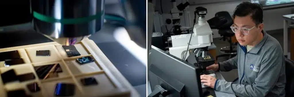
Researchers at Rice University have developed a new nanoscale chip fabrication technique that uses stressed crystals to directly create ultra fine patterns on hard semiconductor materials at room temperature. The breakthrough could simplify the manufacturing of next generation photonic and optoelectronic devices that rely on both electrical and light based signal processing.
The research focuses on alpha molybdenum trioxide, a semiconducting crystal with anisotropic properties, meaning its atomic structure behaves differently depending on direction. When exposed to an electron beam, the crystal naturally deforms, generating highly organized nanoscale ripple patterns. Researchers discovered this stress response could be harnessed to imprint wrinkle like structures directly onto rigid materials such as silica, aluminium oxide, and silicon nitride, all widely used in semiconductor manufacturing.
In the experiment, scientists layered alpha molybdenum trioxide over silica and exposed the structure to an electron beam. While the beam softened the silica surface, the crystal simultaneously buckled under directional stress, transferring organized ripple patterns onto the substrate. These ripples, measuring only hundreds of nanometers wide, function similarly to optical gratings capable of bending, splitting, and guiding light across chips.
Conventional nanoscale wrinkle patterning methods typically require multiple fabrication stages, chemical processing, expensive infrastructure, or flexible substrates. Hard insulating materials usually crack under mechanical stress. The Rice team’s approach overcomes these limitations by enabling one step patterning directly on rigid materials without high temperatures or chemical residue.
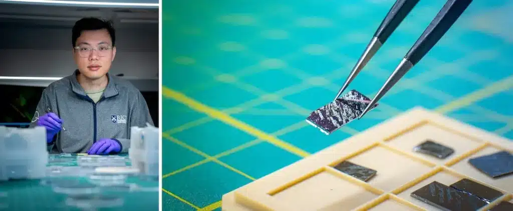
Researchers also found the patterns can be precisely controlled by adjusting the crystal layer thickness or electron beam intensity. Once the process is complete, the crystal layer can simply be peeled away, leaving the patterned surface intact.
Hae Yeon Lee, Assistant Professor of Materials Science and Nanoengineering at Rice University, says “This work is useful because conventional methods for making nanoscale wrinklelike patterns often require many fabrication steps, high cost and chemical processing that can leave residue on the surface of the chip. With our method, the wrinkles are created in one simple step at room temperature.”


