

A Cyprus-based startup has developed a desktop system designed to turn PCB designs into tested working prototypes in about 30 minutes.
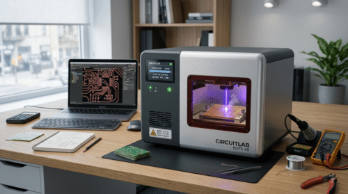
PewCB has introduced the PewCB One, a desktop printed circuit board (PCB) prototyping system intended to let engineers produce and test circuit boards without sending each revision to an external fabrication service. The company says the process, from preparing Gerber files to having a completed board ready for testing, can take about 30 minutes. It positions the system around a Build, Test, Revise and Repeat workflow for faster hardware development.
The machine uses a 1064-nanometre fibre laser with around 20 watts of average optical power, approximately 100-nanosecond pulses and a 35-micrometre spot. Instead of starting with raw copper-clad material, it works with pre-manufactured ceramic PCB blanks containing plated vias and edge through-holes. The laser selectively removes solder mask, copper and substrate material to create the required circuit pattern, avoiding the drilling and electroplating stages normally involved in PCB fabrication. It can also cut a metal stencil for applying solder paste before component assembly. PewCB currently lists support for trace widths and spacing down to 0.1 mm, with compatibility for quad flat no-lead (QFN) packages with 0.5-mm pitch and below and 0402-size passive components.
The desktop approach is intended to reduce the time between making a PCB design and evaluating the resulting hardware. According to PewCB, the system can enable three or more prototype iterations in a working day, allowing engineers to identify problems, modify the design and produce another board without waiting for an external fabrication service.
Early-bird units are priced at $5000 and include the machine and 20 ceramic PCB blanks. PewCB requires a 30 per cent deposit to reserve a unit and gives an estimated delivery period of about 90 days. Shipping, import duties and regional taxes are excluded from the listed price. The company also identifies limitations including potential solder bridging around exposed copper if the stencil is not used correctly, the possibility of ceramic cracking under hard impact and fixed via positions determined by the pre-manufactured blanks.
The PewCB One is therefore aimed primarily at rapid PCB prototyping rather than replacing conventional board fabrication for every application. Its main advantage is the ability to shorten the time between PCB revisions, while the board-size limitations, specialised ceramic blanks and $5000 entry price remain considerations for potential users.