

The system checks PCB solder joints and surfaces, detects solder balls and debris, and reduces board handling during production.
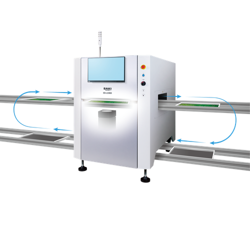
An inline inspection system can check PCB solder joints and the entire board surface from below without requiring boards to be flipped. The 3Di-LS3BX from SAKI Corporation is designed for this task after selective, wave, and dip soldering. It combines 3D inspection of through-hole technology (THT) solder joints with full-surface inspection, reducing manual handling and operator intervention on production lines.
The system addresses inspection requirements in automotive electronics and other applications where reliability is important. Conventional back-end inspection can involve additional board handling and manual checks, increasing production complexity and the risk of damage. Automating these checks can help manufacturers maintain consistent inspection quality and reduce the possibility of human error.
The 3Di-LS3BX uses dedicated THT solder inspection software, proprietary algorithms, and 3D measurement to inspect component pins and solder fillets. Its high-rigidity gantry structure supports stable operation and repeatable results. Standard dome lighting helps capture consistent 3D images of sloped, reflective, and curved surfaces, reducing false inspection calls.
The system also uses SAKI’s Full Memory Technology to inspect solder balls and foreign object debris (FOD) across the entire PCB surface, including unexpected components. It can detect solder balls as small as 200 µm, helping identify potential defects that might otherwise go unnoticed during conventional inspection.
For integration into existing production lines, the 3Di-LS3BX shares its software platform with SAKI’s solder paste inspection (SPI) and post-reflow AOI systems. This provides a common operating environment for inspection workflows across surface-mount technology (SMT) and back-end processes. An optional return conveyor can be installed beneath the system to accommodate different production line layouts.
The system extends automated inspection to the bottom side of PCBs after soldering, complementing inspection processes used earlier in manufacturing.
Click here for the original announcement.