




A millimetre-scale crystalline organic semiconductor film for OLEDs, significantly improving charge transport, reducing operating voltage, and paving the way for brighter, more efficient next-generation electronic displays.
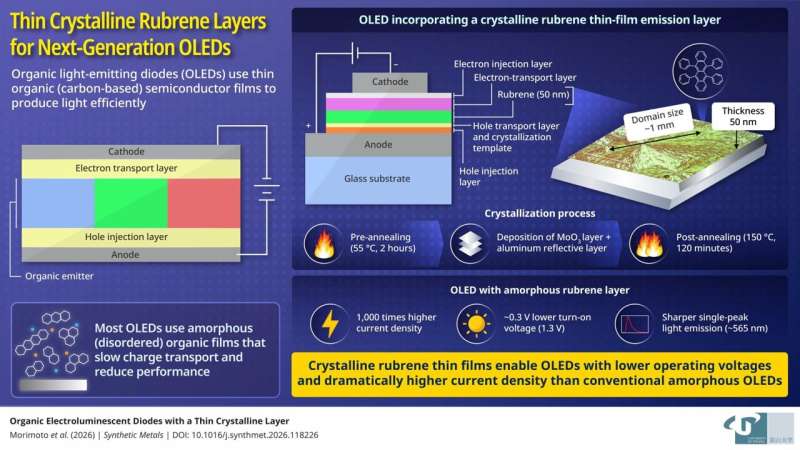
Researchers at the University of Toyama have demonstrated a manufacturing technique that transforms conventional amorphous organic semiconductor films into large crystalline structures, dramatically improving the electrical performance of organic light-emitting diode (OLED) devices. The advance could enable brighter, more energy-efficient displays for smartphones, televisions, wearable electronics and future flexible display technologies.
The advancement centres on rubrene, an organic semiconductor widely known for its excellent charge-transport properties in the crystalline form. In today’s OLED manufacturing processes, rubrene is typically deposited by vacuum evaporation, producing an amorphous film in which randomly arranged molecules impede charge transport. This disorder limits current flow, increases operating voltage and reduces device efficiency.
To overcome this limitation, the research team developed a two-step thermal annealing process that converts a thin 50nm rubrene layer into a highly ordered crystalline film after deposition. During the first heating stage, microscopic crystal nuclei are created within the organic layer. Following deposition of the remaining OLED layers, a second heat treatment promotes crystal growth, forming orthorhombic crystalline domains measuring up to 1mm across far larger than those achieved using conventional fabrication methods.
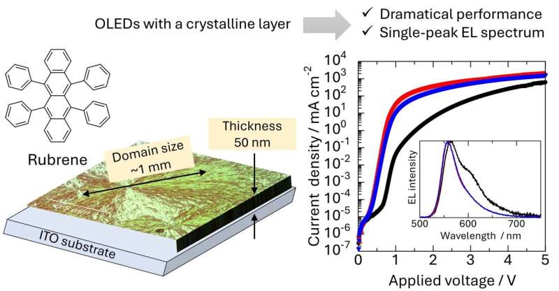
The structural transformation substantially enhances electronic performance. OLEDs incorporating the crystalline rubrene layer achieved current densities up to 1,000 times higher than devices using amorphous films. The luminance turn-on voltage dropped by approximately 0.30V, reaching only 1.33V, indicating significantly lower power requirements for light emission. The devices also produced a sharp single electroluminescence peak near 565nm, replacing the broader dual-peak emission characteristic of amorphous rubrene and confirming the formation of the crystalline phase.
The technique is particularly significant because it is compatible with established OLED fabrication methods rather than requiring entirely new manufacturing equipment. By improving charge transport within organic semiconductor layers, it could increase display brightness while lowering power consumption, extending battery life in portable electronics and improving display efficiency in larger panels.
Beyond consumer displays, the approach could benefit a broader range of organic electronic devices, including flexible displays, organic transistors, sensors and emerging optoelectronic systems. The ability to produce large-area crystalline organic semiconductor films using a scalable post-deposition process addresses one of the longstanding challenges in organic electronics, bringing high-performance crystalline OLEDs closer to commercial production.


