




A lead-free material detects infrared light and can be printed to make sensors for facial recognition, LiDAR, industrial inspection and medical use.
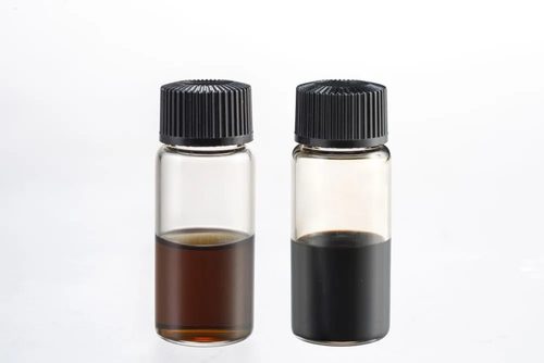
A lead-free quantum dot material has achieved an external quantum efficiency (EQE) of 18.4% in a photosensor detecting short-wave infrared (SWIR) light at wavelengths of 1200–1700nm. Made from silver, sulfur and tellurium, the material can be deposited using printing processes without vacuum processing. It could provide an alternative to conventional infrared detector materials in smartphone facial recognition, 3D sensing, automotive LiDAR, industrial inspection and biomedical applications. Developed by TANAKA PRECIOUS METAL TECHNOLOGIES in collaboration with the Torimoto Laboratory at Nagoya University, Japan, the material contains neither lead nor cadmium.
During performance evaluations, the silver-sulfur-tellurium (Ag-S-Te) quantum dots formed the active layer of a simplified photosensor. Light in the 1200–1700nm range is less susceptible to noise from sunlight and the effects of adverse weather, making it suitable for outdoor sensing. It also offers greater eye safety and can penetrate certain materials and biological tissues.
Infrared sensors are used in wearable devices, industrial inspection cameras and other systems. Indium gallium arsenide (InGaAs), which detects wavelengths up to 1700nm with high sensitivity, is commonly used in these applications. However, its manufacturing process requires vacuum processing, and production yield and cost remain challenges for mass production. Indium supply is also a concern as demand increases for high-speed communication semiconductors in artificial intelligence (AI) data centres, perovskite solar cells and smartphone displays.
Lead sulfide (PbS) quantum dots have been explored as a lower-cost alternative to InGaAs. These semiconductor particles measure a few nanometres, and their light absorption and emission wavelengths can be adjusted by changing their size. They can be deposited using printing processes suitable for large-area production, with sensors reportedly costing approximately one-tenth as much as InGaAs sensors. However, PbS contains lead, which is restricted under the Restriction of Hazardous Substances (RoHS) Directive because of concerns about its effects on human health and the environment. This limits its use in consumer electronics.
The Ag-S-Te material avoids both lead and cadmium while offering a printing-based manufacturing process. TANAKA and Nagoya University are also developing methods to control its composition, particle size and surface properties to customise optical characteristics and compatibility with different manufacturing processes.