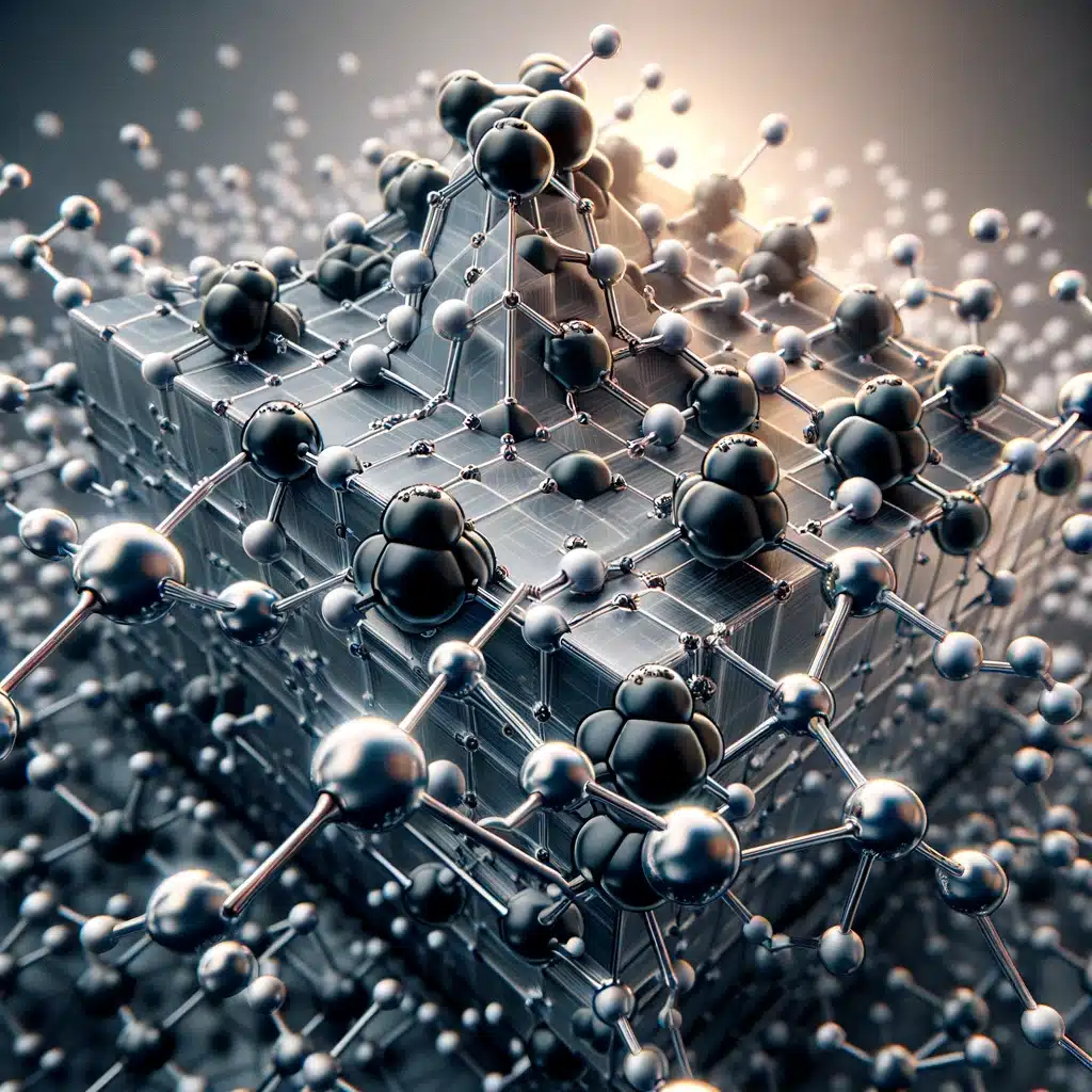
This approach preserves the delicate physical properties of the 2D material.
Researchers at Hunan University, the Chinese Academy of Sciences and Wuhan University recently have developed a novel fabrication method for monolayer black phosphorus (BP) and germanium arsenide (GeAs) transistors using a technique based on van der Waals peeling. This method represents a remarkable innovation in the handling and manipulation of 2D materials.
The development of monolayer transistors using two-dimensional (2D) semiconductors like black phosphorus and germanium arsenide marks a significant breakthrough in the field of scaled electronic devices. The fabrication process for these materials, however, has faced substantial challenges, primarily due to the inherent difficulties in forming stable and robust electrical contacts with these fragile 2D materials.
The van der Waals peeling technique involves a layer-by-layer mechanical peeling process. This method allows the channel region of a multilayer black phosphorus transistor to be gradually thinned down to a monolayer. All this while maintaining the integrity of its delicate lattice structure and retaining a thicker, multilayer contact region. This approach preserves the delicate physical properties of the 2D material, which are essential for the optimal performance of the transistor.

An interesting observation from the utilisation of this technique is the change in the electrical properties of the 2D transistor as the channel thickness varies. It was found that the carrier mobility in black phosphorus decreases significantly when its body thickness is reduced. This behaviour is more akin to that of a conventional bulk semiconductor, rather than a pure van der Waals semiconductor, which often exhibits different electronic characteristics.
The ability to manipulate and study these materials at such a fine scale opens up new avenues for research and development in semiconductor technology, potentially leading to more efficient, smaller, and faster electronic devices. Moreover, the van der Waals peeling technique could be a game-changer in the fabrication of 2D semiconductors, offering a more controlled and less invasive approach to creating monolayer devices.


