Can a common mineral improve quantum materials? Researchers have replaced polymer-based assembly with mica to create cleaner atomic stacks for future electronics.
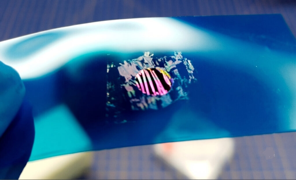
Scientists from the University of Southampton and the National University of Singapore have developed a fabrication technique that uses the natural mineral mica to build ultra-clean two-dimensional (2D) heterostructures. The method is designed to reduce contamination during the assembly of atomically thin materials, improving their suitability for quantum technologies and next-generation electronic devices.
Two-dimensional materials such as graphene and hexagonal boron nitride are known to exhibit new electronic and magnetic properties when stacked with precise angular alignment. These layered structures are widely studied for applications in quantum computing and nanoelectronics. However, conventional fabrication methods rely on synthetic polymer films to transfer and stack the layers, often leaving microscopic residues that affect device performance.
The approach replaces these polymer films with muscovite, a naturally occurring form of mica. Because mica is an inorganic crystal with an atomically flat surface, it enables cleaner transfer of the thin material layers while reducing contamination. The researchers say the method also lowers fabrication costs and provides a more stable surface for accurately aligning individual layers.

Using the mica-based process, the team demonstrated improved control over stacking atomically thin materials, making it easier to produce complex 2D heterostructures for experimental devices. The cleaner interfaces could help researchers better study quantum phenomena, where even small amounts of contamination can influence electronic behaviour and obscure experimental results.

The researchers believe the technique could support the development of future nanoelectronics and quantum devices by enabling more reliable fabrication of advanced material stacks.
“Our new method allows us to precisely align the layers to create these complex structures that were previously too hard to make. This level of precision is vital for quantum material research, where even a tiny amount of contamination can obscure the results,” says Dr Makars Šiškins, Lecturer in Experimental Physics at the University of Southampton.