

A Nanjing Tech team has screen-printed every layer of a perovskite solar cell in ambient air, achieving 22.41 per cent efficiency without vacuum equipment or inert-atmosphere gloveboxes.
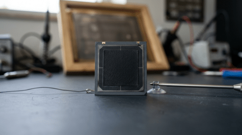
Researchers at Nanjing Tech University have developed a perovskite solar cell in which every functional layer is screen-printed under ambient conditions. The work reports a power conversion efficiency (PCE) of 22.41 per cent, with an independently certified efficiency of 21.86 per cent. The research was carried out at the State Key Laboratory of Flexible Electronics, with collaborators from the Frontiers Science Center for Flexible Electronics and Northwestern Polytechnical University.
Crystallisation has long been a challenge in screen-printed perovskite solar cells. When the ink is deposited in air, crystallisation can begin at the exposed surface before the precursor has properly filled the underlying porous structure, leading to voids and pinholes. The Nanjing Tech team addresses this with a fluid-motion crystallisation strategy based on a co-solvent system containing the ionic liquid methylammonium propionate and butyronitrile. The ionic liquid keeps the perovskite precursors dissolved, while butyronitrile reduces the ink’s resistance to flow, helping it penetrate the porous layers. This changes the crystallisation sequence, allowing the perovskite to undergo an ordered phase transition from the bottom of the scaffold upwards before significant surface nucleation occurs. The researchers report that this produces a dense, interconnected network of perovskite nanocrystals. A carbon electrode is used as the top contact.
The certified 21.86 per cent efficiency is close to the reported 22.41 per cent laboratory value, making the independently verified result more significant than the headline figure alone. The researchers evaluated stability using the international summit on organic photovoltaic stability (ISOS) testing protocols. Under ISOS-L-1 light soaking, the devices retained 90.5 per cent of their initial PCE after 2000 hours. Under the more demanding ISOS-L-3 test, conducted at 85°C and 50 ± 10 per cent relative humidity, the paper reports no measurable degradation after 900 hours.
Many high-efficiency perovskite solar cells are fabricated using laboratory techniques such as spin coating and vacuum-based deposition, which can be difficult to translate directly to high-throughput manufacturing. Spin coating is poorly suited to large-area production because it uses the ink inefficiently, while vacuum evaporation requires additional equipment and can add expensive electrode materials such as gold or silver. The Nanjing Tech process avoids both approaches by screen-printing the functional layers and using a carbon electrode. Screen printing is already an established high-throughput manufacturing technique, making the process more compatible with scalable production. The significance of the result is therefore not just the 21.86 per cent certified efficiency, but the combination of competitive efficiency with an air-processed, fully screen-printed fabrication route.
This is a laboratory demonstration with a certified single-cell result, not a pilot line. The reported efficiency is for individual devices rather than a commercial module, and the study does not establish how the process would perform at large module scale or under outdoor conditions. The work therefore demonstrates the feasibility of fully screen-printed, air-processed perovskite cells rather than a production-ready manufacturing process.
India’s solar-cell manufacturing build-out under the production-linked incentive scheme is dominated by crystalline-silicon technologies, making the manufacturing approach demonstrated by the Nanjing Tech team particularly relevant. Screen printing is already an established process in silicon solar-cell production, including for metallisation, so a fully screen-printed perovskite architecture could potentially reuse parts of an existing manufacturing ecosystem rather than require the same vacuum-deposition infrastructure used by many laboratory perovskite cells. The approved list of models and manufacturers (ALMM) governs eligible solar PV modules for specified government-linked projects, but the treatment of emerging technologies such as perovskite modules should be checked against the latest MNRE requirements before deployment claims are made. IIT Bombay’s NCPRE is also actively working on perovskite-silicon tandem solar cells, including through its TANDEM Laboratory and collaboration with Waaree Energies. India is adding solar-generation capacity considerably faster than it is adding manufacturing depth, so a printing route that avoids vacuum equipment could eventually broaden the range of manufacturers able to produce advanced solar cells.
For more information, click here.