




A compact silicon optical modulator combines slow-light technology with an integrated electro-optic equalizer to achieve 200Gbps transmission, potentially improving bandwidth and energy efficiency in next-generation AI data centres.
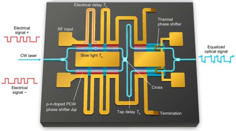
Researchers in Yokohama National University, Japan have demonstrated a silicon optical modulator capable of transmitting data at up to 200 gigabits per second (Gbps), addressing the need for faster, compact and energy-efficient optical interconnects in artificial intelligence (AI) data centres. The device combines a slow-light photonic crystal waveguide with an integrated electro-optic (EO) equalizer, achieving high-speed transmission in a structure measuring just 320 micrometres (µm) in length. The findings, published in Nature Communications, could support denser optical connections between processors and computing accelerators.
Conventional silicon optical modulators convert electrical signals into optical signals but typically require several millimetres of chip space. Improving modulation efficiency while maintaining high-frequency performance remains a challenge, particularly as data centres require increasing bandwidth without proportionally increasing power consumption.
The new design uses a photonic crystal waveguide containing a carefully arranged pattern of microscopic holes that slows light as it travels through silicon. This slow-light effect strengthens the interaction between light and the device, enabling small electrical changes to produce more effective optical modulation. However, the resulting electrical resistance can limit high-frequency operation.
To overcome this limitation, researchers integrated an EO equalizer into the modulator. The equalizer compensates for the device’s declining response at higher frequencies, extending its operating bandwidth. In the demonstrated designs, the frequency response increased from 35 to 80 gigahertz (GHz) and from 23 to 55 GHz. The device was fabricated using a 300-mm silicon-on-insulator manufacturing process, compatible with established semiconductor production techniques.
The modulator achieved 140 Gbps using on-off keying, consuming 26 femtojoules per bit. With four-level pulse-amplitude modulation (PAM-4), it reached 180 Gbps without digital signal processing (DSP). Adding a low-complexity, 11-tap receiver equalizer increased the data rate to 200 Gbps, with energy consumption of 63 femtojoules per bit.
Despite its compact dimensions, the device has an optical insertion loss of 11.7–15.5 decibels, which researchers compensated for using an optical amplifier during testing. Further optimisation is needed before practical deployment. Future integration of 16–32 optical channels could potentially deliver aggregate bandwidth of 3.2–6.4 terabits per second, although this remains a projection rather than a demonstrated result.