A test system checks chiplets before packaging, helping chip makers find faulty chips early, reduce waste, improve yield, and increase processor reliability.
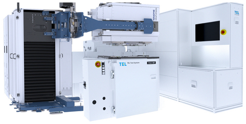
Teradyne has introduced an integrated test cell for known good device (KGD) screening, developed with Tokyo Electron (TEL), to help semiconductor manufacturers detect defective chiplets before they are assembled into advanced AI and data center packages. The solution combines Teradyne’s UltraFLEXplus test platform with TEL’s Prexa Singulated Device Prober (SDP) and is designed for use by fabless chip designers, foundries, outsourced semiconductor assembly and test (OSAT) providers, and integrated device manufacturers during the advanced packaging process.

The system enables users to electrically test individual dies before they are integrated into 2.5D and 3D packages. By identifying faulty dies early, manufacturers can avoid assembling defective chiplets into high-value packages, improving production yield, reducing manufacturing waste, and increasing the reliability of finished AI and data center processors.
The integrated test cell combines electrical testing with thermal control. During testing, the UltraFLEXplus platform evaluates device performance, while the Prexa SDP maintains device temperature and manages the high-power dissipation associated with AI chips. The validated configuration is intended for high-volume manufacturing and reduces the effort required to integrate separate testing and probing systems.
The solution is built on an open architecture that supports different probe cards, manipulators, and interface technologies. It can also be integrated with other compatible testers and probers, allowing manufacturers to adapt the system to their existing production lines.

The commercially available test cell is intended to support known good device screening at multiple stages of the advanced packaging flow, helping semiconductor companies improve package quality and manufacturing efficiency as chiplet-based AI and data center devices become more common.
Click here for the original announcement.