


The process design kits open early access to high-density chip connections, giving you a way to test, build, and push multi-chip systems toward real use cases.
The NanoIC pilot line, led by imec, has released two interconnect process design kits (PDKs) that allow early design of high-density chip-to-chip systems beyond 2nm. These kits give design teams access to tools needed to build and test advanced packaging before full manufacturing support is available.

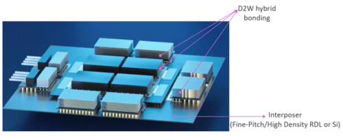
The release includes a fine-pitch redistribution layer (RDL) PDK and a die-to-wafer (D2W) hybrid bonding PDK. Both are aimed at universities, start-ups, SMEs, and industry teams working on next-generation chip systems. They provide design rules, layout support, and validated building blocks so users can start creating and checking designs.
The RDL PDK focuses on routing on polymer-based substrates. It enables smaller interconnect pitches, with line widths and spacing down to 1.3 microns and microbump pitches of 20 microns. This helps improve data transfer speed and reduce energy use in chip-to-chip links, making it useful for computing systems, automotive designs, and GPU architectures.
The D2W hybrid bonding PDK enables direct 3D connections between dies. It removes the need for copper bumps and instead uses oxide-to-oxide bonding between the chip and the package. This reduces signal loss and supports dense, high-bandwidth connections needed in AI and high-performance computing systems.
These PDKs are an early version. They allow designers to build layouts, test routing, and run design checks. Future versions are expected to support full tape-out, where designs can be manufactured and tested on the pilot line.
As chip design moves toward combining multiple dies into one system, packaging now plays a direct role in performance. The way chiplets connect affects speed, power use, and data movement. By releasing these PDKs, NanoIC adds interconnect design to its existing set of tools, which already includes N2, A14, and eDRAM PDKs, forming a broader toolkit for next-generation chip systems.
Click here for the original announcement.