


The new PMMA-InOx hybrid photoresist can pattern with low exposure, has high etch resistance, and offers reliable processing for future semiconductors.
Scientists at the Center for Functional Nanomaterials (CFN) have developed a unique organic-inorganic hybrid material. This new material is sensitive to light and facilitates the creation of high-quality patterns using EUV lithography.

To keep making smaller and more efficient semiconductor devices for the next generation of electronics, we rely on advanced techniques like extreme ultraviolet lithography (EUVL). However, this method faces challenges, such as the need for better EUV photoresists that are sensitive, can create sharp patterns, and can withstand etching processes.
This material, made of poly(methyl methacrylate) (PMMA) combined with indium oxide (InOx), is created using a method called vapor-phase infiltration (VPI). VPI is a way to make hybrid materials that come from a process similar to atomic layer deposition.
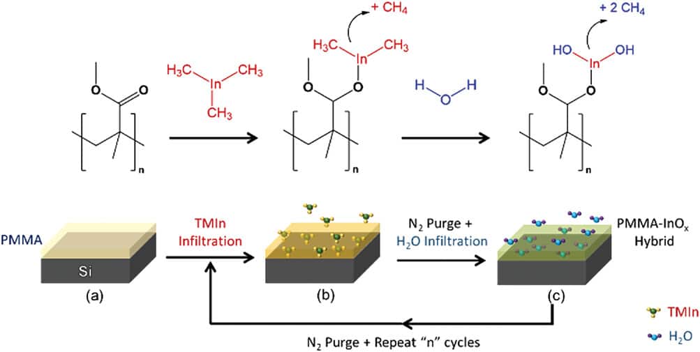
The advantage of using a gaseous form of indium, known as trimethylindium, is that it binds weakly to the PMMA and allows the inorganic part to spread evenly throughout the material. This even spread helps the photoresist perform well under EUVL and electron-beam lithography (EBL), allowing for detailed patterning at low energy levels (18mJ cm^2 for EUVL and 300µC cm^2 for EBL).
For example, it can create very fine line patterns that are only 40 nanometers wide and hole patterns with 50 nanometers diameter, while also being highly resistant to etching by silicon, by a factor of over 30 to 40 times.
“One of the main problems we encountered when initially making these hybrids is that the inorganic content needs to be uniformly distributed inside the organic polymer while making sure that the infused inorganic components are not too strongly bound to organic matrix,” said Ashwanth Subramanian, the lead author of the paper.
Center for Functional Nanomaterials (CFN) is a U.S. Department of Energy (DOE) Office of Science user facility at DOE’s Brookhaven National Laboratory. As a national scientific user facility, the CFN provides users a research experience supported by top-caliber scientists and with access to state-of-the-art instrumentation.
