


High-speed inter-chip (HSIC) interface is becoming more popular due to its notable advantages over USB for hard-wired inter-chip applications. The interface is a two-signal, source-synchronous interface that can provide USB high-speed data at 480Mbps. Data transfers are 100 per cent host-driver compatible with traditional USB topologies. Full-speed (FS) and low-speed (LS) are not supported by the format. However, a hub with HSIC can provide FS and LS support.
The interface differs from USB in the physical layer only. Significant features include no chirp protocol, source-synchronous serial data transmission and no hot removal or attach as the interface is always connected.

It has 1.2V signal levels designed for low-power applications at standard LV CMOS levels. Maximum trace length is 10cm. The protocol for data transactions between host and device via HSIC is the same as USB, as shown in Fig. 1.
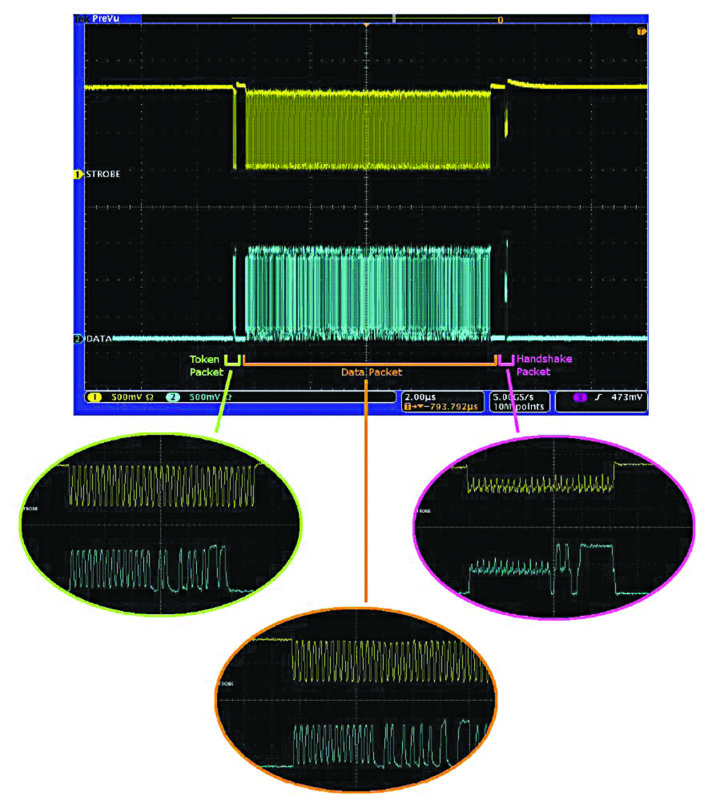
The primary difference between the two is that in HSIC all information is transmitted via a single data line, and a strobe signal communicates when to sample the received data signal. HSIC uses double data rate (DDR) signalling; data are sampled at both the rising and falling edges of the strobe signal. The strobe signal oscillates at a frequency of 240MHz, which provides a total data rate of 480Mbps.
Advantages of HSIC over USB
HSIC has significant advantages over USB. For a start, it is a fully-digital standard and, thus, no analogue frontend is required. Lack of an analogue frontend means die sizes can be reduced and, thus, so can the cost. Additional die reduction can also be made due to the decreased amount of digital logic required by the simplified connection protocol.

HSIC standard does not inherently reduce power consumption, but removal of the analogue frontend can lead to lower-power designs, especially since analogue circuitry does not necessarily scale one-to-one with digital circuits for reductions in process feature size.
HSIC is especially low-power when placed into the suspended state as there is no current drawn on the strobe or data lines. By comparison, standard USB draws a minimum of 200µA on D+ through a 1.5kΩ pull-up resistor when suspended.
Because HSIC is only different from USB at the physical layer, migrating from USB to HSIC is not like changing to a completely new standard. This means existing USB software stacks and USB protocol knowledge bases can be quickly transitioned to HSIC.
Data sampling
With standard USB, every data packet begins with a sync pattern to allow the receiver clock to synchronise with the phase of incoming data. The differential sign of D+/D- signal is then sampled according to the sync pattern. HSIC uses a separate strobe line to tell the receiver when to sample incoming data. HSIC data signal is sampled at the rising and falling edges of the strobe signal. If the strobe and data signals become skewed for any reason, sampled data may become corrupted. HSIC Electrical Specification defines the maximum allowable skew as 15ps.
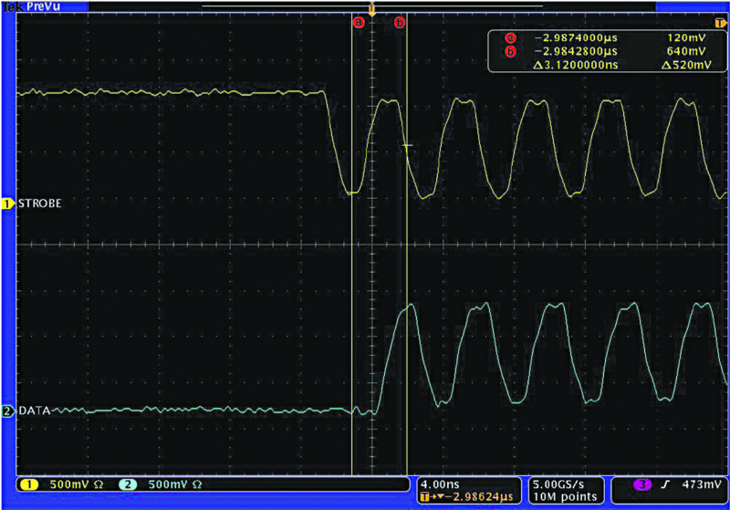
To make sure the skew does not become an issue, HSIC traces must be kept as short as possible and must not be longer than 10cm. Data and strobe traces must be the same length, and these should be routed to 50Ω single-ended impedance.
To illustrate the amount of skew possible in the real world, Fig. 2 shows the beginning of a test packet transmitted from a host to a device with equal lengths.
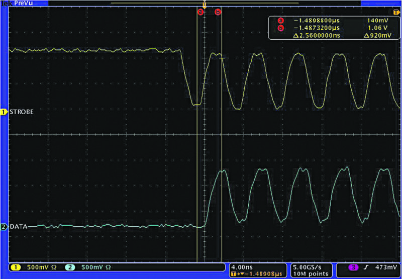
The same packet transmitted from the same host with a strobe trace that is about 10cm longer than the data trace is shown in Fig. 3. The resulting skew is about half of a nanosecond. This is an extreme example, but results suggest that even a small amount of length mismatch may result in an HSIC specification violation.
The single-ended nature and differences in signal termination cause some difficulties when attempting to probe HSIC lines. Standard USB signals can be easily monitored and deciphered by placing a differential probe connected to an oscilloscope at either the transmitter side or the receiver side. HSIC signals are more sensitive and, thus, transmission line theory should be considered when attempting to probe these.
A good general guideline is to probe at the side opposite to the source of the signal that needs to be observed. For instance, to observe the signals originating from a device, place a probe at host-side terminals. To observe the signals originating from a host, place the probes at device-side terminals.
When attempting to probe signals originating from a device while probing at the device side, the signal becomes distorted. This is likely due to the interference caused by the signal reflecting back on itself. The middle of the trace can also be probed, but results are typically not as clean as if probed properly from one side. The ideal would be to probe simultaneously from both ends. A series protocol analyser may be able to sample the signals accurately in both directions, but the 10cm trace length restriction makes this option impractical.
Making the connection
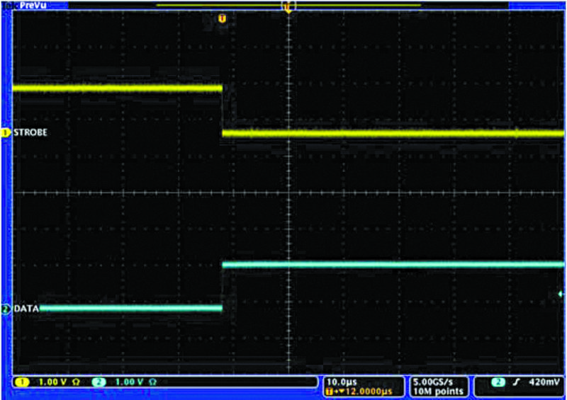
HSIC interface is structured such that a host or peripheral can be powered on in any order. To ensure a false connection is not detected, the host, hub and peripherals must ensure that the strobe or data lines do not float to an undetermined value, commonly referred to as tri-stated.
Fig. 4 shows an oscilloscope capture of a connect sequence. This connect sequence is much simpler than the USB connect sequence because there are no speeds to negotiate. This sequence can be handled by a very simple state machine, reducing die size requirements.
With standard USB, the host can determine if a downstream port has been disconnected by monitoring the magnitudes of DP/DM signal voltages. If the voltage exceeds the disconnect voltage threshold, the host can conclude that the device has been disconnected.
HSIC does not support a disconnect protocol because it is intended to be a hard-wired, always-on connection. However, it is still possible to have a situation where a downstream device may appear to have disconnected, and care must be taken to ensure the host does not permanently lose its connection with the device.
This apparent disconnection or standoff can occur because the host always maintains an idle state while the bus is unused, and the idle state is identical to the suspend state from a signal perspective. The host has no way of knowing if or when a downstream device has been powered down or disconnected. Since the suspend signalling is identical to the idle signalling, it is possible to reach a state where a downstream device believes it has been suspended while the upstream host thinks there is no device downstream and waits indefinitely for a connect signal to arrive. A similar standoff condition could occur if the upstream host disables the port while the device believes it has been suspended.
This condition is not likely to occur between hosts and devices that never cycle power or soft reset. If this issue is encountered, it must be dealt with in an application-specific manner at either the link or software-stack level. This can be done by programming the software stack or designing the link in a way that prevents the condition from occurring in the first place.
Alternatively, the system(s)-on-chip (SoC) can attempt to deal with a downstream device after it disconnects by resetting HSIC hub. The device discovery sequence will occur, and the connection will be re-established.
On Microchip’s USB254x, USB3613, USB3813, USB4604 and USB4624 devices, the SoC can use VBUS_- DET pin to re-establish the connection. Pulling the pin low suspends the hub, while pulling the pin high wakes it up.
Conclusion
HSIC standard has advantages over USB in hard-wired applications as long as the correct connection and disconnection procedures are observed. These procedures are particularly important when troubleshooting some issues involving HSIC connectivity.
