


Making computer chips is becoming harder, slower, and more expensive. A new way of generating light could help the semiconductor industry move beyond some of today’s
most stubborn manufacturing limits.
Modern chipmaking is increasingly an exercise in managing bottlenecks. Today’s leading manufacturers rely on extreme ultraviolet (EUV) lithography, which uses 13.5nm light generated by firing powerful lasers at tiny droplets of tin. Once produced, this light must pass through a complex system of 11 mirrors before reaching the wafer. Each mirror reflects only about 70% of the light, meaning 30% is lost at every step. Because each reflection introduces loss, only a small fraction of the original light ultimately reaches the wafer surface. That reduced usable light directly affects wafer throughput and contributes to the high cost of advanced chip production. Think of it like trying to pass a bucket of water through 11 people in a line, where some water spills at every handoff. By the time it reaches the end, only a small amount is left for the actual job.
Mirror loss, however, is only one of several constraints. EUV light generation itself remains inherently inefficient, while wafer materials require extremely precise exposure control: too little light prevents accurate pattern formation, too much can destroy the wafer. As feature sizes continue to shrink, optical systems also demand increasingly sophisticated mirror architectures and tighter tolerances, driving cost and engineering complexity even higher.
Because EUV operates at a fixed 13.5nm wavelength, further scaling cannot rely on changing the light itself. Instead, it requires increasing the system’s numerical aperture (NA), which in turn demands larger, more complex, and more precise mirrors—further compounding cost and engineering difficulty. It is similar to trying to read smaller and smaller text using the same pair of glasses. If the lens power cannot be changed, the only option is to build a much larger, more precise lens system.
Taken together, these challenges suggest that conventional EUV lithography is approaching practical limits in efficiency, scalability and cost. This raises a bigger question for the industry: Is there a way around these limits, or is chip manufacturing approaching a fundamental ceiling?
Breaking down the new approach
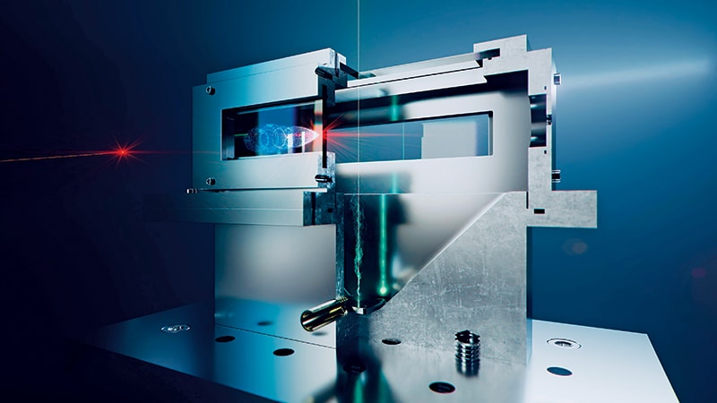
One emerging approach changes how the lithography light itself is produced. Instead of relying on plasma-based EUV sources, it uses a laser-plasma accelerator—a compact particle accelerator driven by ultra-short, high-intensity laser pulses. These pulses generate plasma waves that trap electrons and accelerate them to very high energies over just a few millimetres, rather than the much larger footprints associated with conventional accelerator systems. Imagine giving a sprinter such a powerful push at the starting block that they reach full speed in a few steps instead of needing an entire track.
The accelerated electrons then pass through an undulator, a carefully engineered sequence of alternating magnets. As the electrons oscillate through this magnetic structure, they emit highly coherent EUV or soft X-ray light in a free-electron-laser-style architecture. Unlike conventional EUV sources, this light is tunable, allowing the wavelength to be better aligned with mirror designs and photoresist response windows used in photolithography.
Unlike EUV systems fixed at 13.5nm, this architecture is not fundamentally wavelength-capped. By adjusting electron energy and undulator design, shorter wavelengths can be generated, positioning the platform not just for the next node, but potentially for multiple future node generations.
So, basically, instead of being stuck with a single piano key, this system can play across a whole keyboard, choosing the exact note needed for each future generation of chip design.
This coherence is one of the most important differences from current systems. Because the emitted light behaves more like a laser beam than an incoherent plasma source, the optical design can eliminate large light-collection optics and use a more compact mirror pathway. The result is lower delivery loss, improved usable brightness at the wafer plane, and the potential for faster wafer exposure. It is the difference between using a torch that shines in one focused direction versus a lantern that scatters light everywhere.
Although the source and beam-delivery path are new, the approach is designed to preserve as much of the downstream scanner architecture as possible. Most notably, the wafer-scanning and positioning subsystems, the precision mechanisms responsible for overlay accuracy, and pattern placement, can remain largely unchanged. This improves the technology’s potential compatibility with existing fab workflows, even though full process integration and requalification would still be substantial industrial tasks.
The shorter usable wavelength range also opens a path to continued scaling beyond current EUV approaches, potentially reducing dependence on increasingly complex multi-patterning strategies. Importantly, this advantage is not solely about wavelength; it also depends on resist chemistry, defect control, and overlay precision, all of which remain critical to achieving future sub-2nm-class process nodes.
Beyond lithography, the same accelerated electrons can also generate X-rays before entering the undulator. These X-rays could support advanced inspection, metrology, and 3D imaging of multilayer chip structures, adding potential value in semiconductor quality control. It is a bit like getting both the printing tool and the inspection camera from the same machine.
From lab to fab
The accelerator platform is compact enough to fit within a standard shipping container-sized footprint and consists of three primary stages. First, an infrared laser generates ultra-short pulses that create plasma in a gas medium, accelerating electrons. Second, magnetic beamline systems shape and stabilise the electron bunches across space, timing, and energy spread. Finally, the electrons pass through the undulator to generate coherent EUV or X-ray light, which is then directed toward the scanner using high-reflectivity mirrors. Throughout the system, thermal management, vibration isolation, and stabilised mirrors keep the beam steady, ensuring precise chip patterning.
Although the light source is new, the wafer-scanning system can remain largely unchanged. The goal is to integrate the system with existing machines with minimal modifications, particularly to the wafer-scanning components that handle precise positioning. The setup would resemble current implementations: the container-sized system sits below the fab floor near the scanner, and mirrors direct the X-ray or XUV light to the wafer.
The largest engineering challenge has been converting what was once a lower-repetition-rate laboratory technology into a continuously operating industrial platform. This requires stable electron bunch generation, precision beam shaping, automated controls, and long-duration operational consistency. A key factor in this transition is increasing the pulse repetition rate of the system. Higher repetition rates directly translate into more exposure events per second, making repetition rate a critical lever for achieving competitive wafer throughput in high-volume manufacturing. The repetition rate works much like a high-speed printer: the more pages it can print per second, the more work it gets done in an hour.
Industrial adoption will depend on reaching competitive high-volume manufacturing throughput targets—roughly 100-250 wafers per hour—and sustaining that performance with maintainable uptime. Reaching this level remains one of the key milestones between prototype success and fab deployment.
The tough road to faster chips
The central challenge in next-generation compact X-ray and EUV sources is generating high-energy electrons inside a small system while maintaining component integrity, beam stability, and industrial reliability. Laser-driven acceleration helps address this by supporting electric field strengths far beyond those achievable in conventional accelerator architectures, enabling rapid acceleration in a much smaller footprint.
Even so, system integration and cost remain major hurdles. While the optical chain may reduce dependence on some of the large, highly specialised collection optics associated with today’s EUV systems, new cost centres emerge in ultra-short-pulse lasers, beamline controls, magnetic systems, stabilisation hardware, and maintenance infrastructure. The long-term economic case will therefore depend on the total cost of ownership rather than on optics-only savings.
Energy efficiency is another promising advantage, particularly through efforts to improve wall-plug-to-X-ray conversion efficiency and recover part of the system’s unused energy. While not all losses are practically recoverable, improving this conversion pathway could significantly reduce electricity consumption per wafer over time. Similar to regenerative braking in electric vehicles, some of the wasted energy is captured and reused rather than lost as heat.
The broader industry context also matters. Existing high-NA EUV systems have long deployment lifecycles and enormous installed cost bases, meaning that adoption of any alternative architecture will likely be gradual. Rather than replacing current EUV systems immediately, this approach is strategically positioned to enable the generation of beyond-high-NA tools. As the industry explores even higher numerical apertures, sometimes referred to as hyper-NA, the associated cost and complexity are expected to rise sharply, creating an inflection point where a new light-source architecture becomes more viable.
The strongest case for this next-generation approach lies in its ability to improve performance while avoiding the escalating complexity associated with ever-larger optics and greater dependence on multi-patterning.
Building the future
The platform is designed for scalable deployment, with one compact light source paired to each scanner, an architecture that aligns well with how current fabs already provision lithography tools. Rather than depending on a massive centralised accelerator feeding multiple scanners, the system can be deployed closer to individual tools, simplifying beam delivery and reducing facility-level integration complexity. Instead of one giant power station serving an entire city block, this works more like placing a dedicated generator next to each building.
A major focus is improving wall-plug efficiency: maximising the conversion of electrical power into usable lithography light at the wafer plane. This includes optimised laser design, reduced optical losses, and partial energy-recovery strategies.
The first near-term applications are outside semiconductor lithography, where commercialisation cycles are shorter, and reliability can be proven faster.
One early target is space radiation testing, where compact accelerator systems can improve access to high-energy particle environments used to validate electronics for orbit. Another is medical therapy, particularly very-high-energy electron-based cancer treatment, where compact accelerator footprints could make advanced treatment systems more affordable than large proton installations.
These adjacent applications serve an important strategic role: they function as real-world validation environments for cost efficiency, power efficiency, uptime, and maintainability. That operational proof can later strengthen the platform’s readiness for semiconductor fab integration. In practical terms, these markets serve as real-world proving grounds before the technology is trusted in the semiconductor industry’s most demanding production lines.
Jerome Paye is Chief Executive Officer of TAU Systems. He brings extensive leadership experience in product development, program management, manufacturing, and operations across North America and Europe.
Co-author Nidhi Agarwal is Senior Technology Journalist at EFY.