


While semiconductor diode lasers, or simply laser diodes, are extensively used in a range of laser devices intended for tactical military applications, such as short and medium-range laser rangefinders, proximity sensors, short-range laser dazzlers and laser aiming devices, it needs to be emphasised here that they are invariably used as the optical pumping source for all Nd:YAG laser-based military systems.
Laser-diode electronics primarily comprises a constant-current source that can provide to the forward-biased laser diode the desired magnitude of current and also has in-built features to provide protection to the device against all those parameters it is adversely sensitive to. The other important circuit block is the temperature controller that can maintain the laser diode junction at the desired value of constant temperature irrespective of ambient temperature. The need for a precise constant-current source and constant-temperature operation arises from the dependence of laser-diode wavelength on drive current and operating temperature. Not all laser-diode applications, including military applications, have stringent requirements of ultra-stable wavelength necessitating a high degree of current and temperature stabilisation, though for efficient and reliable operation, stability of drive current and operating temperature are always desirable.

Although laser diodes exhibit excellent reliability under ideal operating conditions, these are highly susceptible to damage due to excessive drive current, electrostatic discharge (ESD) and transients. Laser diode damage manifests itself in the form of one or more of the following problems, namely, reduced output power, shift in threshold current and increase in beam divergence and failure to laser action, thus producing an LED-like output only.
Relevant damage mechanisms are overcurrent, overheating, current spikes and power-line surges. Improper grounding and shielding lead to radiated electrical transients. Improper power-line conditioning also leads to severe fast transients. ESD caused by improper handling during storage, transport and mounting is considered as the single leading cause of premature laser diode failure.
Constant-current and constant-power operational modes
There can be two possible circuit topologies the laser diodes can be operated in, namely, constant-current and constant-output power modes. Operating temperature is of course an important factor in both the modes. In view of dependence of laser diodes’ performance on operating temperature and drive current, the preferred mode of their operation is the constant drive current with precise control of operating temperature. Constant-current operation without temperature control is generally not desirable. Even at constant drive current, output power would increase with decrease in operating temperature. With significant decrease in temperature, output power could easily go past the absolute maximum value.
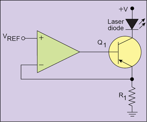
The circuit topology in the case of constant-current mode of operation is usually configured around a current- sensing element that continuously senses the drive current and produces a proportional voltage. This is then compared with a reference voltage representing the desired value of drive current to generate an error signal. The error signal, after suitable conditioning, is fed back to restore the drive current to the desired value. Fig. 1 shows the basic schematic arrangement of constant-current drive circuit.
Practical circuits with in-built protection features are far more complex. Typical constant-current drive circuits and related design issues are discussed in the following paragraphs.
There are applications where constant output power is more relevant. In such a situation, direct dependence of output power on drive current can be exploited to maintain a constant output power. Even when a laser diode is driven by a constant current, the heat dissipated at the laser-diode junction leads to rise in temperature and hence fall in output power. Increase in temperature could be because of absence of any active temperature control mechanism or even inadequacy of heat sink in the presence of active temperature control.
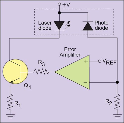
This reduction in output power can be compensated by increasing the drive current. The current source can be designed in such a way that it adjusts the drive current in a feedback mode to maintain a constant output power instead of maintaining a constant drive current. Fig. 2 shows the basic circuit topology. The basic circuit topology of constant-output- power drive circuit is similar to that of constant-current drive circuit, except for the nature of sense signal, which in the present case is a photo current proportional to the output power.
grounded load
circuit for floating load
Constant-output-power drive circuit needs to be operated with an absolute current limit to prevent any thermal runaway problem caused by uncontrolled increase in drive current. Laser diode modules with an integral photodiode (Fig. 3) facilitate constant-output-power operation, though noise intrinsic to the integral photodiode manifests itself in the form of noisy and unstable output in the case of constant-output-power mode of operation. The device usually has three terminals, including either anode or cathode of laser diode, either anode or cathode of photodiode and a common terminal obtained by connecting the remaining terminals of laser diode and photodiode. In some cases, all four terminals, two of laser diode and two of photodiode, are brought out.
Laser-diode drive circuit: constant-current mode
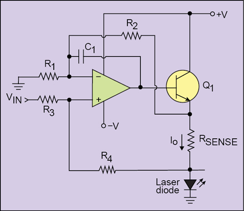
Fig. 4 shows the basic constant-current source circuit for grounded-laser-diode configuration. Laser-diode current is sensed differentially by measuring voltage across RSENSE wired in series with laser diode. Laser diode current in this case can be computed from IO = VIN×R4/(R3×RSENSE), where R1 = R3 and R2 = R4. C1 is the compensation capacitor connected for stable operation. VIN may be derived from a band-gap reference. In case the control voltage VIN is of negative polarity, it is connected to R1 and R3 and is grounded instead. A digitally-controlled current source may use a voltage output digital-to-analogue converter to generate VIN.
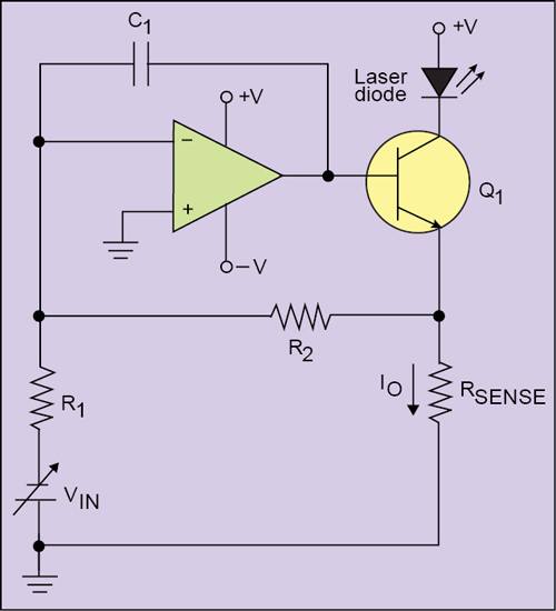
Similar circuit for a floating load is shown in Fig. 5. Laser-diode current in this case can be computed from IO = VIN×R2/(R1×RSENSE).
diode driver for OEM applications
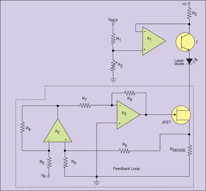
The voltage-controlled constant- current sources discussed so far provide constant-current drive to the laser diode, provided the DC supply voltage, the voltage at the emitter terminal and the resistance in the emitter lead were all constant. It would be a reasonably good assumption if the source voltage were derived from a precision band-gap reference and the resistors used had stability specifications equal to or better than the desired level of current stability. But when it comes to achieving a higher level of current stability, say ±10ppm or better, a feedback loop that in situ samples the diode current and applies a correction in the case of drift in drive current becomes essential. A negative feedback loop of this kind would reduce the drift or error in the drive current by a factor that equals the loop gain.
One such circuit is shown in Fig. 6. The basic circuit topology is similar to the one used in driver circuits described in the previous pages. The only change is inclusion of a junction FET (JFET) connected in series with the sense resistor and wired as a voltage variable resistor. A small variation in drive current is compensated by an appropriate variation in the drain-source resistance of the JFET.
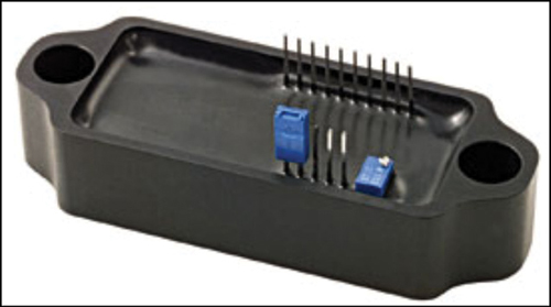
Initially, at the nominal value of drive current, circuit parameters are so adjusted as to ensure that JFET with the feedback loop closed gets a negative gate voltage to keep it nearly in the middle of its VVR characteristics. This is done to fully exploit the voltage-dependent resistance range. Precision constant-current laser diode drivers are commercially available today from a host of manufacturers for original equipment manufacturer (OEM) applications. A representative photograph is shown in Fig. 7.
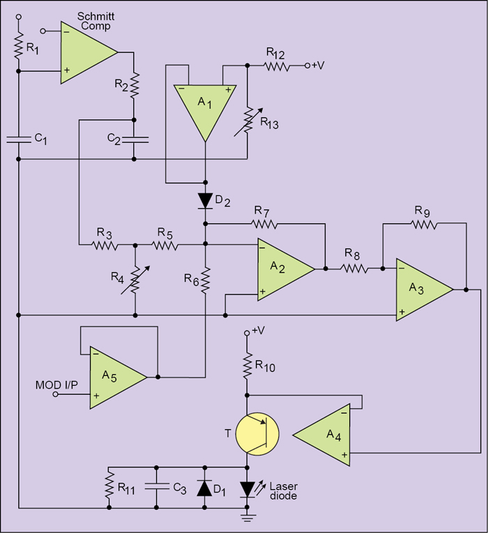
Protection features, such as slow start, immunity to fast transients and overcurrent limit, as outlined earlier, are essential features for every laser diode driver circuit to have. Fig. 8 shows a constant-current laser diode drive circuit with modulation capability and in-built above-mentioned protection features.
Let us first talk about protection features provided by the drive circuit. The Schmitt comparator at the input provides a delay of the order of a few tens of milliseconds after the switch-on to offer protection against switch-on transients. The time delay is decided by the R1C1 time constant. R2 and C2 provide the desired slow or soft start and decay during switch on and switch off. R2C2 time constant is of the order of one to two seconds. R11 and C3 provide additional protection against transients; D1 protects the laser diode against reverse voltages.
The constant value of drive current is decided by the voltage present at the noninverting input of op-amp A4, which equals the voltage present at the output of op-amp A2, provided R8 = R9. This is further equal to sum of voltage levels due to modulation input and reference voltage VR after potential divider constituted by R3 and R4 and also assuming that R5 = R6 = R7. This is true only if voltage V after potential divider arrangement R13 and R14 and appearing at output of op-amp A1 did not interfere. This is true as long as diode D2 is reverse biased, which it is during normal operation.
If the drive current exceeds a certain preset limit governed by voltage at the output of op-amp A1, diode D2 gets forward biased and clamps the voltage at the noninverting input of op-amp A4 to the voltage at the output of op-amp of A1, thereby providing overcurrent limit. The circuit may be modified to include a JFET and associated feedback loop components as shown earlier in Fig. 6 to improve current stability.
Laser-diode drive circuit: constant-output-power mode
multi-stage
TE modules
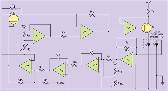
Laser diode can be driven to maintain a constant-output power by varying the drive current in accordance with the output power. The feedback loop circuit is such that it increases or decreases the drive current in response to decrease or increase in output power. Fig. 9 shows the constant-output- power drive circuit. The integral photodiode produces current proportional to optical output power from the laser diode. This photocurrent is converted into a proportional voltage using a transimpedance amplifier configured around op-amp A4.
The voltage representative of laser power is then summed up with a reference voltage representing the desired power level in an inverting summer configuration A5. The output of the summer, which is null when the actual power level equals the desired power level, feeds integrator A6 that provides the correction signal even for infinitesimally small deviations from the desired power level. The integrator output summed up with a bias voltage feeds control element, which is a junction FET in this case.
The drive current, and hence the output power, is governed by voltage present at noninverting input of op-amp A3. Evidently, reduction in laser- diode-output power causes reduction in photodiode current, which finally leads to gate terminal of JFET becoming more negative. This further causes a reduction in voltage at A3 noninverting input, increasing the drive current to restore the output power. Similarly, increase in laser-diode power reduces drive current to restore the power at nominal value.
Driving laser diode in pulsed mode
There are two possible modes of operation of laser diodes to produce a pulsed output. In one of the operational modes of relevance to their use in military devices, such as laser rangefinders employing time-of-flight principle and laser proximity sensors, the laser diode is driven by current pulses that are a few tens to a few hundreds of nano-seconds wide. In the other operational mode, called quasi-CW mode, laser diode is driven by current pulses that are typically hundreds of microseconds to a few milliseconds wide. This operational mode is invariably used in the case of laser-diode arrays pumping solid-state lasers, including those for military rangefinders, target designators, electro-optic countermeasures and so on.
Quasi-CW operation of laser diodes for optical pumping of solid-state lasers is at relatively low repetition rates of typically a few hertz to a few tens of hertz. This allows them to be operated at relatively high peak powers, which is made possible due to low duty cycle of operation of quasi-CW devices, which keeps the average power low.
An important consideration while designing laser-diode drive circuits for pulsed operation, conventional or quasi-CW operation, the laser diode(s) must not be switched between cut-off and the nominal maximum value. This is highly detrimental to the life of laser diodes. They must always be operated between lower values slightly greater than the lasing threshold and the nominal value. Laser diode driver circuits for conventional pulsed and quasi-CW operation are configured around the same basic building blocks as those described earlier in the case of CW operation. The laser diode drive circuit of Fig. 8 can be used for operation in conventional pulsed mode by applying the desired pulsed waveform at the modulation input. The lower value of drive current is governed by R3-R4 potential divider.
half-bridge circuit
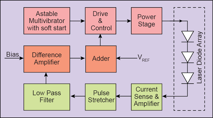
In the case of quasi-CW operation of laser diode arrays used for optical pumping of solid-state lasers, peak- current-pulse amplitude typically varies from a few tens to a few hundreds of amperes. The current drive stage in this case is usually a cascade arrangement of a drive and control stage and a power stage. Drive and control stage is a preamplifier stage with some kind of control feature that allows to vary the amplifier gain and hence the drive current to the power stage. Fig. 10 shows the block schematic arrangement of a typical quasi-CW laser-diode drive circuit.
The circuit operates as follows. The astable multivibrator produces a train of pulses having pulse width and repetition rate at which the laser diode or laser-diode array needs to be driven. Soft start in-built into the circuit provides protection against damage due to instant power on. Power stage contains the active device(s) and associated circuitry capable of delivering required current pulse amplitude.
The drive and control stage could be configured either around discrete bipolar transistors/metal-oxide-semiconductor field-effect transistors (MOSFETs) or an op-amp with JFET as one of the gain determining elements. The power stage could be configured around one or parallel connection of more than one bipolar transistors or MOSFETs. The sensing element is usually a resistor connected in series with the diode or diode array. The peak pulse voltage across the sense resistor representing the peak amplitude of current pulse is amplified and then subsequently stretched. The stretched pulse train, after filtering, is fed to a differential amplifier stage where it is compared with a standard reference to produce an error voltage. The error voltage here represents deviation of peak amplitude of current pulse from the desired value. The error voltage is added to a fixed bias and fed to the control element in the drive stage to control the drive current to the power stage.
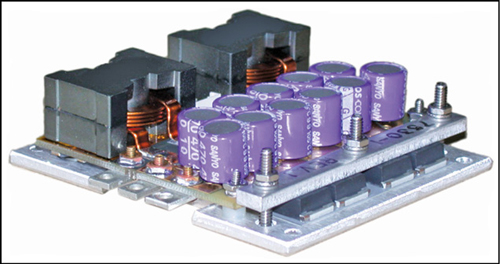
Again, a large number of manufacturers internationally offer compact laser-diode drivers for OEM market catering to the requirements of CW, conventional pulsed and quasi-CW operational modes. Fig. 11 shows photograph of one such laser-diode driver for quasi-CW operation. One cannot miss the bank of capacitors connected across the DC supply input to provide high peak current drive capability required in such an operation.
Laser diode temperature control circuits
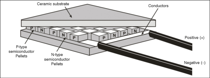
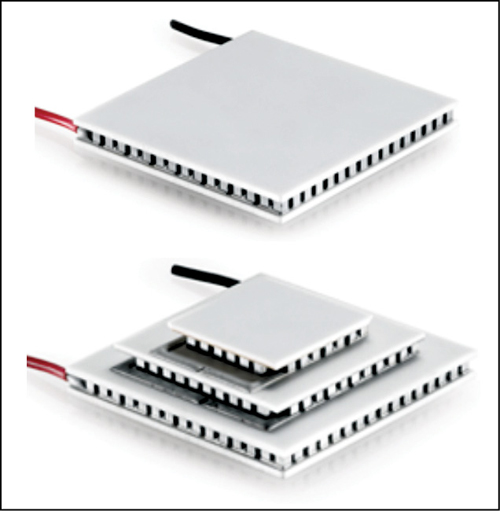
Laser diode junction gets heated due to power dissipated at the junction, and one of the methods to remove heat away from the junction is by using a heat sink. This passive technique of heat removal using heat sink becomes impractical for moderate-to-large power-diode lasers. Also, it cannot be used to operate the laser diode at a temperature lower than the ambient temperature, nor can it be used to stabilise the temperature. Use of an active temperature stabilisation mechanism therefore becomes essential while working with moderate-to-high-power-laser diodes and also in low-power laser diodes where application demands precise temperature control. Thermoelectric (TE) cooling device based on Peltier effect is the heart of such a system. A practical TE module is usually a two-dimensional array of P-N couples connected electrically in series and sandwiched between two thermally conducting and electrically insulating faces (Fig. 12). Both single-stage and multiple-stage TE cooler modules (Fig. 13) are commercially available. Multiple-stage modules offer higher cooling/heating capacity and maximum differential temperature specifications.
TE-cooler-based active temperature stabilisation circuit uses TE module as the control element, a temperature sensor and a properly designed feedback loop. The TE cooler is a reversible solid-state heat pump whose operation is based on the Peltier effect. According to the Peltier effect, when electric current is passed through a junction of dissimilar metals, heat is created or absorbed at the junction, depending upon the direction of flow of current. The heat transfer according to the Peltier effect takes place in the direction of flow of charge carriers.
A TE module literally pumps heat from one place to another, heating one face and cooling the other in the process. Whether a particular face becomes hot or cold depends upon the direction of current flow through the TE module. Thus, by controlling the magnitude and direction of the current drive to the TE module, it can be used as a control element in a temperature stabilisation circuit. The TE module pumps the heat dissipated in the laser diode on to a heat sink mounted on the supposedly hot face of the TE module. The heat is transferred from heat sink to the ambient.
TE modules are characterised by maximal performance parameters, namely, maximum temperature difference ΔTMAX at zero heat load, maximum heating capacity QMAX for zero temperature difference, device currentIMAX measured at ΔTMAX, terminal voltage VMAX corresponding to IMAX with no heat load and coefficient of performance (COP), which is the ratio of pumped heat load to electrical power supplied to the device.
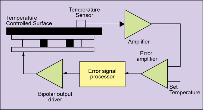
Fig. 14 shows the basic block schematic of TE-module-based temperature control circuit. Key building blocks of the drive and control circuit include temperature sensor, error amplifier, error signal processor and a bipolar output drive circuit. Bipolar output driver provides the required power to drive the TE module. The output stage in most cases is designed to allow flow of drive current in either direction through the TE module. This enables both cooling and heating of the device to maintain its temperature at the specified value, regardless of ambient temperature being higher or lower.
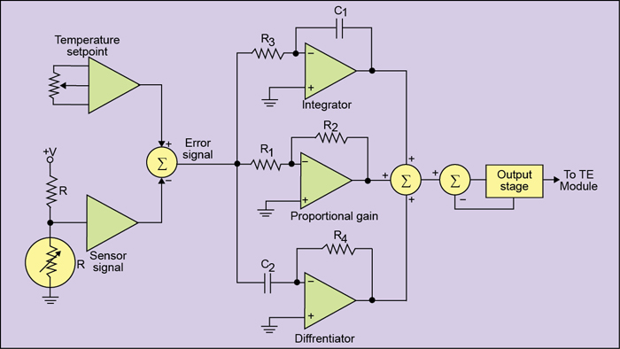
Negative temperature coefficient (NTC) thermistor is the most commonly used temperature sensor due to its high sensitivity. RTD and semiconductor sensors have better linearity but suffer from poor sensitivity. Semiconductor sensors are also available in integrated circuit form producing a current linearly related to absolute temperature. AD 590 is one such sensor. Balanced bridge circuit configuration that generates a differential output is generally used. Error amplifier is configured around an op-amp. Error-signal processor could be anything from simple on-off controller to a proportional controller or proportional-integral (PI) or even fully digital PI-differential (PID) controller.
On-off controller is never used in practice. In proportional control, the drive signal to the TE module is proportional to the difference between the actual and desired temperatures. In a proportional controller, there is always a residual error even after the controller has settled to the final state. This error is proportional to the difference between the desired and the actual temperature and is inversely proportional to the gain of the control loop.
The problem of residual error of a proportional controller can be overcome by the addition of an integrator in the control loop. The result is a PI controller. One disadvantage of PI control is that it would be slow to respond to large residual errors. PID overcomes this problem encountered in PI controllers. Addition of derivative term improves the loop’s transient response. This type of controller is mainly used in applications where large thermal loads must be controlled rapidly and accurately. Fig. 15 shows a typical PID controller interfaced with other building blocks, including temperature sensor, reference generating circuit and error amplifier.
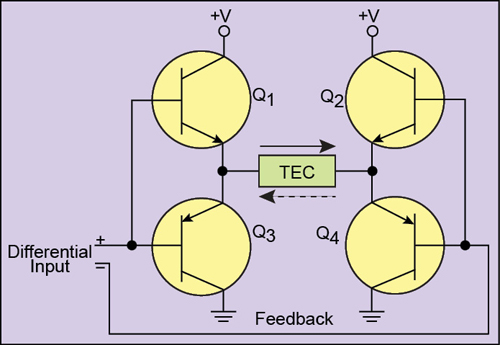
The output stage provides necessary drive power to the TE module. In most cases, electronic systems are designed to operate from a single positive DC voltage supply. Also, in most applications, TE modules need to be driven in bipolar mode to cater for both heating and cooling operations. A commonly used circuit topology to provide bipolar drive to TE modules while operating from a single DC voltage is the half-bridge circuit topology (Fig. 16). The circuit is usually driven at the input by a driver amplifier stage with a differential output. Transistors Q1-Q4 and Q2-Q3 conduct alternately to provide bidirectional operation of TE module. A cascade connection of two half-bridge circuits may be used to enhance voltage and current drive capability of the output stage.
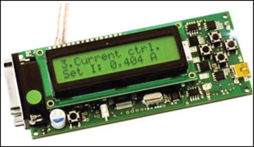
TE drive and control modules for laser diode temperature control and stabilisation are commercially available, both as general-purpose benchtop equipment as well as for OEM applications. Even integrated-laser-diode drive and temperature-control modules are available for OEM applications. Fig. 17 shows a representative photograph.
Present-day military laser rangefinders and target designators are largely configured around diode-pumped pulsed solid-state lasers. We have discussed in the preceding paragraphs the building blocks of laser-diode drive and temperature-control electronics. Circuit topologies of laser-diode drivers for different modes of operation of laser diodes, including CW, quasi-CW and pulsed modes and also laser-diode temperature drive and stabilisation, have been discussed. Gas laser electronics is in focus in the concluding part of the article.
To be continued in the fourth part
Dr Anil Kumar Maini is a senior scientist, currently the director of Laser Science and Technology Centre, a premier laser and optoelectronics research and development laboratory of Defence Research and Development Organisation of Ministry of Defence. Nakul Maini is a technical editor with Wiley India Pvt Ltd