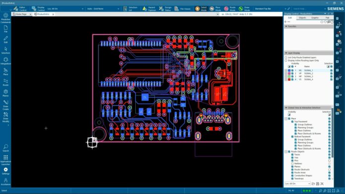

Design, verify, collaborate, and prepare complex PCBs for manufacturing with a professional EDA platform built around constraint-driven design, automation, 3D verification, and system-level collaboration.
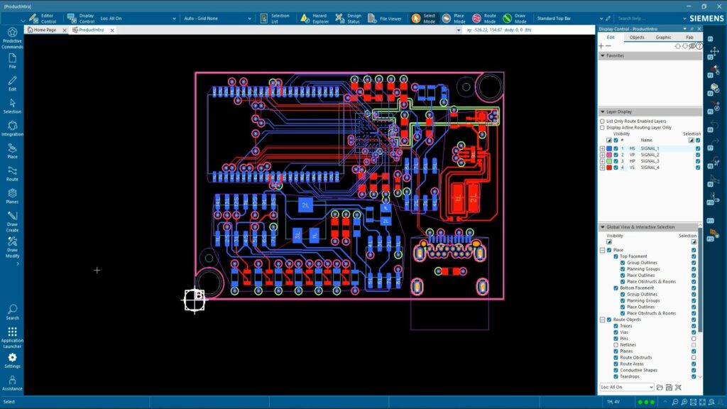
Designing a PCB is much more than drawing tracks between components. As boards become denser and faster, engineers must simultaneously consider signal integrity, component placement, power delivery, thermal and mechanical constraints, manufacturability, and the relationship between the PCB and the rest of the electronic system. Siemens Xpedition is designed for this kind of complex electronic system development.
Xpedition is a professional electronic design automation (EDA) platform focused primarily on PCB and electronic-system design. It brings together schematic design, component and library management, constraints, PCB layout, routing, 3D design, verification, collaboration, and manufacturing-oriented workflows. Instead of treating each stage as an isolated activity, the platform connects design information across the development process.
For a beginner, the simplest way to understand it is to think of it as a digital workspace in which an engineer can take a board from electrical intent to physical implementation and verification. The engineer can create or modify a schematic, define design constraints, transfer the design into PCB layout, place components, route connections, check the board, inspect it in 3D, collaborate with mechanical engineers, and prepare data for manufacturing.
The software is particularly relevant when a PCB becomes too complicated for basic layout tools. High-speed interfaces, dense component placement, multi-board systems, RF designs, complex power distribution, mechanical restrictions, and large engineering teams all increase the value of a connected PCB design environment.
What Can You Do With Xpedition?
It provides capabilities across several stages of PCB development. Engineers can use it to:
- Schematic capture and editing for complex electronic designs.
- PCB layout creation with component placement and signal routing, including high-speed designs.
- Design constraint management to ensure electrical, mechanical, thermal, and manufacturing compliance.
- Reuse of proven circuits, layouts, and design blocks to speed development.
- Centralized component library and 3D model management.
- 3D PCB visualization and ECAD-MCAD collaboration for mechanical integration.
- Design-for-manufacturing (DFM) checks and automated validation before production.
- Generation of manufacturing outputs and project documentation.
- Support for RF/PCB co-design and enterprise-level collaborative design workflows.
This makes it different from a simple PCB drawing application. Its purpose is not only to help an engineer create the board but also to maintain design intent and engineering information throughout the development process.
How Does it Help Engineers?
One of the biggest advantages of a professional EDA platform is constraint-driven design. Engineers do not have to wait until the PCB is finished to discover that a particular spacing, routing, or connectivity requirement has been violated. Design rules and constraints can guide the layout process itself.
This becomes important in high-speed electronics, where routing is influenced by requirements such as differential-pair behaviour, length matching, impedance and spacing. Similarly, dense boards may require careful consideration of component clearances and mechanical interfaces.
It also focuses heavily on design reuse. Instead of recreating a circuit or layout section that has already been tested, engineers can reuse established design information. For organisations working on multiple products or product generations, this can turn previous engineering work into reusable design knowledge.
Another benefit is the connection between electrical and mechanical design. PCB engineers can exchange information with MCAD teams so that board-level changes and mechanical changes can be reviewed before they become expensive manufacturing problems.
Who Can Use Xpedition?
It is primarily aimed at professional engineering environments rather than casual PCB experimentation.
| User | How it can help |
| PCB designers | Create layouts, place components, route signals, manage constraints, and verify boards |
| Electrical engineers | Capture schematics, define electrical intent, and work with PCB implementation |
| High-speed design engineers | Manage demanding routing and signal-related constraints |
| RF engineers | Work with RF and PCB design data through supported co-design workflows |
| Hardware teams | Collaborate across schematic, PCB, mechanical, and manufacturing stages |
| System engineers | Define and verify requirements across complex electronic systems |
| Large engineering organisations | Manage design data, collaboration, reuse, and controlled workflows |
For students and beginners, it can still be useful for learning professional PCB workflows, but it is important to understand that the software is feature-rich and aimed at serious engineering work. A beginner who has only used basic PCB tools may initially find the environment overwhelming.“The Xpedition tools enabled us to do several things we weren’t able to do with our old solutions, including easy and fast routing of differential pairs, integrated manufacturing data via ODB+, detailed constraint definition, and iteration between engineering and PCB design departments,” said one user.
Design Workflow
The exact workflow depends on the product tier and engineering environment, but a simplified PCB development process looks like this:
1. Define the design
The engineering team establishes the electrical requirements and design intent.
2. Create the schematic: Components are selected and connected to represent the electrical behaviour of the system.
3. Define constraints: Requirements relating to connectivity, spacing, routing, and other physical or electrical characteristics are established.
4. Prepare libraries: Symbols, footprints, package information, and 3D models are associated with the components.
5. Move into PCB layout: The schematic connectivity becomes the basis for physical PCB implementation.
6. Place components: Components are positioned according to electrical, mechanical, thermal, and manufacturing considerations.
7. Route the PCB: Signals are connected while observing the defined constraints. Differential pairs, tuning, and other advanced routing requirements can be handled as necessary.
8. Verify the design: Design rules and other verification processes identify potential problems.
9. Check the physical assembly: The 3D environment helps engineers examine component placement and mechanical relationships.
10. Prepare for manufacturing: Design information and manufacturing-related outputs are prepared for the next stage of the product-development process.
The advantage of such an integrated workflow is that design decisions made early can remain connected to downstream verification and manufacturing activities.
What Is New in Xpedition?
The Xpedition 2604 release, introduced in April 2026, is particularly interesting because Siemens is pushing the software beyond conventional PCB CAD with AI assistance, improved multi-board verification, better 3D checking, manufacturing integration, and a more connected design environment.
- AI Support Inside the Design Environment
One of the most notable additions is AI-enabled support assistance. Engineers can ask natural-language questions directly within Xpedition and receive answers based on the documentation and knowledge-base material associated with the product and version being used.
For beginners, this could be one of the more useful changes because learning a professional EDA platform often involves spending considerable time searching documentation. Instead of leaving the application to find information, the engineer can ask a question within the product environment.
- Multi-Board Interface Signal Matching
It adds a multi-board interface signal matcher that helps engineers verify interface I/O, power and ground connections across boards. It can use signal-name matching and dictionaries to identify genuine interface errors while reducing false positives. This is increasingly relevant as products move from a single PCB toward systems containing multiple interconnected boards.
- Earlier Creepage Checking
The layout editor now supports initial validation of creepage clearances. Both online and batch checking are available, allowing engineers to identify potential spacing problems earlier in the layout process.
- Better Manufacturing Documentation
A major addition is the integration of BluePrint for documentation generation. The aim is to produce more accurate manufacturing instructions directly from design information, reducing the possibility of outdated or inconsistent documentation reaching manufacturing.
- IPC-4761 Via-Type Support
Xpedition 2604 also adds native IPC-4761 via-type definition in the pad-stack editor. This information can flow into Valor NPI for manufacturing analysis, creating a closer connection between the PCB designer’s intent and downstream DFM verification.
- Better 3D and Collaboration Workflows
The release also improves 3D model management, component exploration, placement planning and collaboration notes. Web-based check-in/check-out functionality through EDM further extends the connected design workflow.
The recent releases show a clear shift toward improving usability, automation, AI assistance, collaboration, and system-level design capabilities. Xpedition 2510 enhanced the user experience with context-aware commands, faster schematic operations, improved differential-pair handling, hierarchical cross-referencing, and stronger 3D-aware library management. It also improved ECAD-MCAD collaboration through IDX 4.0 and 5.0 support, along with better constraint reuse and enterprise data management. For RF and PCB co-design, it introduced a file-based Keysight ADS Board Link workflow that allows circuit and PCB information to be exchanged without requiring both applications on the same machine.
Xpedition 2504 focused on usability, AI-assisted engineering, and cloud-connected workflows, including an AI-powered chat interface for analysing component datasheets using indexed datasheet content. Earlier, Xpedition 2409 introduced a more modern user experience with AI and cloud capabilities, while improving auto-routing, design reuse, tuning, complex-via handling, and requirements management. Overall, these releases show Xpedition evolving beyond traditional PCB layout toward a more automated, intelligent, collaborative, and connected design environment covering design, verification, manufacturing, and system-level engineering.
Is There a Free Version?
It is not a completely free EDA package. Siemens offers different levels of the Xpedition technology. Xpedition Standard is positioned as a cost-efficient professional PCB design environment for smaller teams and is currently listed by Siemens at an annual price of $2,999. For users who only need to inspect designs, Siemens offers Xpedition Viewer Community, which is free. It provides browser-based viewing of schematics and 2D PCB layouts, PDF viewing, measurements and one GB of cloud storage. More advanced functions such as cross-probing, design comparison and markup are available in the Standard Viewer tier. This distinction is important:
- Xpedition Viewer Community = free design viewing and review
- Xpedition Standard = professional PCB design
- Xpedition Enterprise = advanced enterprise and multi-domain workflows
Therefore, a student or beginner who simply wants to explore an Xpedition design can start with the free viewer, but someone who wants to create and edit complete PCB designs needs an appropriate paid Xpedition product.
Advantages and Limitations
Its biggest advantage is its depth. It is designed to support complex PCB and electronic-system development rather than just basic board layout.
- Professional PCB design capabilities
- Constraint-driven design
- Advanced routing and layout functions
- Strong 3D design and verification capabilities
- ECAD-MCAD collaboration
- Design reuse
- Multi-board and system-level capabilities
- AI-assisted support and engineering workflows
- Manufacturing and DFM integration
- Enterprise collaboration and data management
- RF/PCB co-design capabilities
- Regular feature updates
The limitations include:
- The learning curve can be significant for newcomers.
- The full professional environment is not free.
- Some advanced capabilities are dependent on product tier.
- Beginners may need training and time to understand the complete workflow.
- The depth of the software can make simple PCB projects feel unnecessarily complicated.
- User experiences with interface usability and documentation vary.
The smaller learning curve introduced through recent UX improvements and AI assistance is therefore significant. Siemens itself has been modernising the Xpedition interface since the 2409 generation, with the stated goal of making the environment more intuitive and reducing barriers for new users. One design engineer mentioned that “Using Xpedition, we were able to successfully shorten design time while maintaining uncompromised quality”.
Is it Worth Learning?
For someone just starting PCB design, Xpedition may not be the easiest first tool. A beginner can learn fundamental PCB concepts using simpler tools before moving into a professional platform. However, engineers interested in high-speed digital systems, complex boards, advanced electronics, RF hardware, automotive electronics, aerospace systems, industrial equipment, or large-scale product development can benefit from understanding how a professional EDA workflow works.
The most interesting part of modern software is not one particular routing feature. It is the direction of the platform. Recent releases increasingly connect AI, design reuse, requirements, PCB layout, 3D verification, mechanical collaboration, manufacturing, and enterprise data. For beginners, that means there is a lot to learn. For experienced engineers, it means the same platform can potentially support much more of the electronic product development process. In short, it is not the tool you choose simply because you want to draw a PCB. It is the kind of platform you choose when the PCB itself has become part of a much larger engineering problem.
For more information, click here.