


Cont. from : FPGAs in Data Centres Part 1
Catapult cloud field-programmable gate array (FPGA) architecture accelerates both cloud services (such as search engine) and the Azure cloud platform; Azure is an open, flexible, enterprise-grade cloud computing platform. The reconfigurable Catapult fabric is embedded into each half-rack of 48 servers in the form of a small board with a medium-sized FPGA and local dynamic random-access memory (DRAM) attached to each server. FPGAs used in Catapult servers are central to delivering better Bing results. These can quickly score, filter, rank and measure the relevancy of text and image queries on Bing.

Catapult v2 design is more flexible in circumventing traditional data centre structures for machine learning and expands the role of FPGAs as accelerators. It expands the availability of FPGAs, allowing them to be hooked up to a larger number of computing resources. FPGAs are connected to DRAM, central processing unit (CPU) and network switches. These can accelerate local applications, or act as a processing resource in large-scale, deep-learning models. Much like with Bing, FPGAs can be involved in scoring results and training deep-learning models.
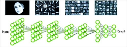
Fig. 16: Deep learning
Catapult v2 design can be used for cloud-based image recognition, natural language processing and other tasks typically associated with machine learning. It could also provide a blueprint for using FPGAs in machine learning installations. Many machine learning models are driven by graphical processing units (GPUs), but the role of FPGAs is less clear. FPGAs can quickly deliver deep-learning results, but consume too much power if not programmed correctly. These can be reprogrammed to execute specific tasks, but that also makes them one-dimensional. In comparison, GPUs are more flexible and capable of handling several calculations.
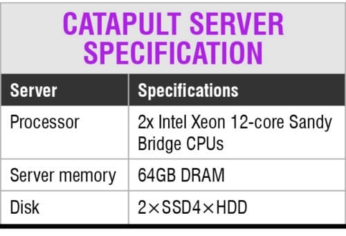
Catapult server specification
Project Catapult employs an elastic architecture that links FPGAs together in a 6×8 ring network that provides 20Gbps of peak bidirectional bandwidth at sub-microsecond latency. It allows FPGAs to share data directly without having to go back through the host servers. It can reprogram the Catapult fabric to adapt to new ranking algorithms without the time and cost of developing custom ASICs or the disruption of having to pull servers from production to install new ASICs—a primary consideration when operating cloud-scale data centres.
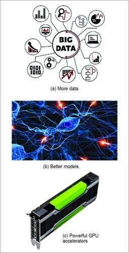
Fig. 17: Drivers for deep learning
Microsoft is putting FPGAs on PCI Express networking cards in every new server deployed in its data centres. FPGAs handle compression, encryption, packet inspection and other rapidly changing tasks for data centre networks that in six years have jumped from Gbps to 50Gbps data rates. In comparison, GPUs are typically more power consuming and more difficult to program.
Power9 processors use Nvidia’s NVLink to connect to chips like Pascal as well as IBM’s own CAPI to link to FPGAs from Xilinx. Separately, ARM will use its Coherent Hub Interface to link to Xilinx FPGAs and other accelerators. The x86 giant is already showing packages that contain Xeon server and Altera FPGA die. It aims to put both the chips on a single die as early as next year. Both CPUs and FPGAs require a lot of power. Putting the two in one socket will limit performance to the thermal envelope of the single chip.
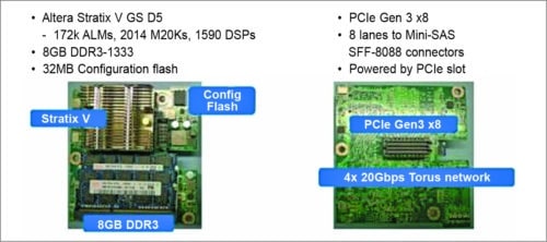
Fig. 18: Altera vs PCI
Microsoft is using Altera FPGAs both in its networking cards and as accelerators for its Bing search. China server vendor Inspur is trying to ride the GPU train with a server packing 16 graphics processors. The server uses a message passing interface the company created for the Caffe deep learning framework developed at U.C. Berkeley for use with GPU accelerators. FPGAs accelerate the ranking of search terms—a new partition of the overall search job.
A special embedded core makes the FPGA more programmable. China’s Baidu has developed an FPGA board accelerating at least ten low-level tasks. The PCIe 2.0 card uses a Xilinx K7 480t with 4GB memory.
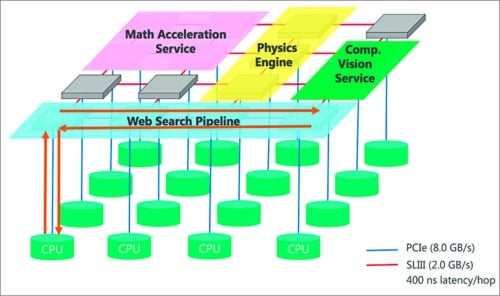
Fig. 19: Catapult uses a network of directly linked FPGAs
Speedster 22i FPGAs built on Intel’s advanced 22nm process technology implement all of interface functions as hardened IP. This results in lower power consumption, reduced programmable logic fabric, faster clock rates, and simpler design since the interface IP is already timing-closed.
Achronix Accelerator-6D board is said to offer the highest memory bandwidth for an FPGA-based PCIe form factor board. This PCIe add-in card is well suited for high-speed data centre acceleration applications. The Accelerator-6D packs a Speedster22i HD1000 FPGA with 700,000 lookup tables, which connects to six independent memory controllers to allow up to 192GB of memory and 690Gbps of total memory bandwidth. Accelerator-6D board comes with a power supply, one-year licence for Achronix ACE design tools, and multiple system-level reference designs for Ethernet, DDR3 and PCIe operation.
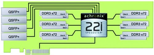
Fig. 20: The Accelerator-6D PCIe form-factor accelerator board (Source: Achronix)
Companies are collaborating on the specification for the new Cache Coherent Interconnect for Accelerators (CCIX). A single interconnect technology specification will ensure that processors using different instruction-set architectures (ISAs) can coherently share data with accelerators and enable efficient heterogeneous computing, significantly improving compute efficiency for servers running data centre workloads. CCIX will allow these components to access and process data irrespective of where it resides, without the need for complex programming environments. This will enable both off-load and bump-in-the-wire inline application acceleration while building on existing server ecosystems and form factors, thereby lowering software barriers and improving the total cost-of-ownership of accelerated systems. CCIX will enable a new breed of high-density, flexible platforms for accelerating compute, storage and networking applications.
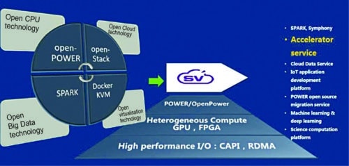
Fig. 21: SuperVessel platform
Intel has presented the future of Xeon processors with integrated FPGAs in a single-package socket compatible to the standard Xeon E5 processors. FPGAs provide users with a programmable, high-performance coherent acceleration capability to turbo-charge their critical algorithms. Algorithms can be changed as new workloads emerge and compute demands fluctuate. The new hardware combination could deliver over 20 times performance gains compared to more traditional ASIC-based solutions.
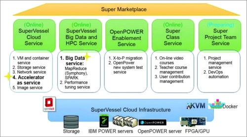
Fig. 22: SuperVessel roadmap
Reprogrammable FPGAs play a central role, enabling a more flexible infrastructure with software-defined allocation and prioritisation of virtualised computing, networking and storage resources. In effect, each FPGA acts as a node controller, for different algorithms to be accelerated across different FPGAs as shared resources in a data centre.
FPGAs allow users to tailor compute power to specific workloads or applications. Xilinx has added support for the proposed interface to its 16nm UltraScale+ product plans, combining its programmable logic with High Bandwidth Memory (HBM) and new accelerator interconnect technology for heterogeneous computing. Built on TSMC’s chip-on-wafer-on-substrate process, Xilinx HBM-enabled FPGAs will improve acceleration capabilities by offering ten times higher memory bandwidth relative to discrete memory channels. HBM technology enables multi-terabit memory bandwidth integrated in a package for the lowest latency.
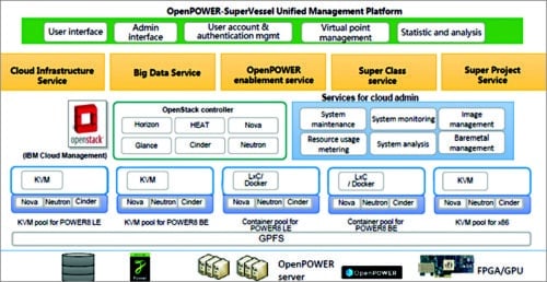
Fig. 23: SuperVessel architecture
Vineyard employs widely used data analytics frameworks such as Spark that make it easier for cloud users to access accelerators.
IBM’s SuperVessel cloud platform, built on top of Power/OpenPower architecture technologies, provides remote access to all the ecosystem developers. Built on OpenStack, the cloud enables:
1. Latest infrastructure-as-services, including PowerKVM, containers and docker services, with big endian and little endian options
2. Big data service through collaboration with IBM big data technology for Hadoop 1.0 and open source technology for Hadoop 2.0 (Spark service)
3. Internet-of-Things application platform service which has successfully incubated several projects in healthcare, smart city, etc
4. Accelerator-as-service (FPGA virtualisation) with the novel marketplace, through collaboration with Altera
In SuperVessel platform, FPGAs and GPUs provide acceleration services, while OpenStack manages the whole cloud.
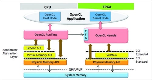
Fig. 24: OpenCL flow
Programming
OpenCL flow allows code written in the increasingly popular parallel-friendly GPU-inspired C dialect to be targeted to Altera FPGAs. Xilinx, on the other hand, has been showing a broader play. For hardware engineers, Vivado is a comprehensive suite of design, analysis and implementation tools.
SDAccel development environment supports OpenCL, C and C++ for software engineers using FPGAs. It enables up to 25 times better performance/watt for data centre application acceleration leveraging FPGAs. High-level synthesis (HLS) provides maximum benefit from the FPGA’s hardware programmability.
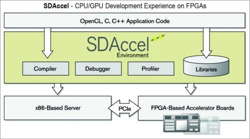
Fig. 25: SDAccel environment
Altera’s OpenCL implementation creates what one might think of as a GPU on an FPGA—with processing elements analogous to GPU cores that execute software kernels in parallel. This solution is easy to program, as it mimics many elements of a GPU, but doesn’t achieve the same performance and quality-of-results as Xilinx’s HLS-based approach. HLS has been repeatedly shown to deliver hardware architectures on par with what skilled experts can create with hand-coded, manually-optimised RTL.
HLS can quickly generate the RTL code, which synthesises down into your chosen architecture. But encapsulating all that power into something that appears to software engineers as a ‘compiler’ is a substantial task.
HLS supports several languages (C, C++ and OpenCL), all at the same time, with the same implementation back-end. There are certainly vast application areas that use C and C++ rather than OpenCL. In order to create a ‘software-like’ development and runtime environment, several pieces of the normal FPGA flow had to be improved.
First, for testing and debugging code, the normal HLS, logic synthesis, place-and-route, timing-closure and device programming cycle would be far too clunky for the rapid-iteration development software engineers are accustomed to. To get around this, Xilinx created a software environment that would be comfortable to any Eclipse-using programmer, and then set up their HLS tool to spit out software-executable cycle-accurate versions of the HLS architecture. This allows the ‘accelerated’ algorithm to execute completely in software for debug and testing purposes, without the long logic synthesis and place-and-route runs required for the final hardware-based implementation.
To get around the run-time issues, Xilinx deployed their partial-reconfiguration technology. This allowed the FPGA to be re-configured with a different algorithm without interrupting system execution. This is critical in data centre applications where a server cannot be arbitrarily taken offline in order to process a normal, full-FPGA configuration cycle. Partial reconfiguration allows the FPGA to keep its inputs/outputs live and to keep some baseline communication with the applications processor while it quickly swaps in new acceleration bitstreams. If the software development and deployment environment is good enough to realise even a fraction of that potential in the data centre, it could represent the biggest revolution ever in managing data centre power.
Emerging algorithms are gaining traction in a wide variety of pattern-matching jobs, from serving up Facebook news feeds to piloting self-driving cars. FPGAs are enabling new types of servers to execute massive bitwise operations in parallel. Analytics servers can replace hundreds of contemporary servers. Microsoft’s data centres drive services like Cortana and Skype Translator, and the company is constantly looking to upgrade server performance. Microsoft is also working with Intel to implement silicon photonics, which will replace copper wires with fibre optics for faster communication between data centre servers.