Imaging sensors are an important component of a wide range of defence systems and are projected to play a growing role in the coming years. This article discusses CCD, CMOS and Ladar sensors in detail.
Two most common types of imaging sensors with potential military applications include charge-coupled device (CCD) sensors and complementary metal-oxide semiconductor (CMOS) sensors. Ladar sensor, which employs a two-dimensional array of avalanche photodiodes, is another important imaging sensor that finds application in precision-guided weapon seeker systems.
Both CCD and CMOS types of sensors use a two-dimensional array of thousands to millions of discrete pixels. The amount of light falling on each of the pixels generates free electrons with the number of electrons and hence the quantum of charge depending upon the intensity of impinging photons. These sensors differ in the mode in which this charge is converted into voltage and subsequently read out of the chip for further processing.

Charge-coupled device
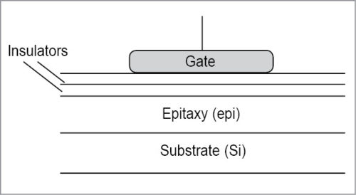
Charge-coupled devices (CCDs) are basically an array of thousands to millions of light-sensitive elements called pixels etched onto a silicon surface. Each of the pixels is a buried-channel MOS capacitor.
CCDs are typically fabricated on a p-type substrate and a buried channel is implemented by forming a thin n-type region on its surface. A silicon dioxide layer is grown on top of the n-type region and an electrode, also called gate, on top of the insulating silicon dioxide completes the MOS capacitor. The electrode could be metal, but is more likely to be a heavily doped polycrystalline silicon conducting layer (Fig. 1). The sensor is not actually flat, but has tiny cavities (like wells) that trap the incoming light and allows it to be measured. Each of these wells or cavities is a pixel.
The size of CCDs is specified in mega-pixels. Megapixel value can be computed by multiplying number of pixels in a row by number of pixels in a column. For example, 1000 pixels in a row and 1000 pixels in a column make 1.0-megapixel CCD chip.
When the light reflected off the target to be imaged is incident on the array of pixels, the impinging photons generate free electrons in the region underneath the pixels. In order to make sure that these free electrons don’t combine with holes and disappear as heat energy, the electrons underneath each pixel are held there by applying a positive bias voltage to the pixels.
If the sensor array were exposed to light for the same time, the number of electrons and hence the quantum of charge held under a certain pixel would vary directly as per the luminous intensity that particular pixel is exposed to. This charge pattern represents the light pattern falling on the device. The charge is read out by suitable electronics and then converted into a digital bit pattern that can be understood and stored in a computer. This digital bit pattern then represents the image.
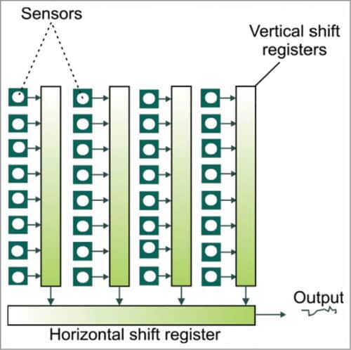
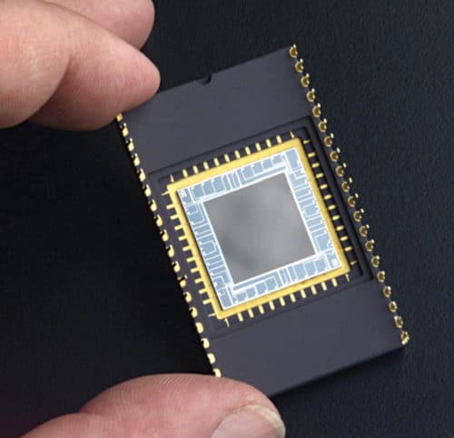
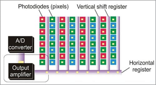
The charge held in bins corresponding to different pixels is read out, converted into equivalent analogue voltages and then digitised with the help of an analogue-to-digital converter. Charge on a CCD is shifted in two directions: parallel (or horizontal) and serial (or vertical). While parallel shift occurs from right to left, serial shift is performed from top to bottom and directs charge packets to the measurement electronics. One way to make the read-out process faster is to split up the image into two or four different sections. Each section follows the process of parallel and serial shift. Fig. 2 shows a typical CCD sensor with a single-point read-out. Fig. 3 shows a typical packaged CCD chip.
The CCD sensor described in previous paragraphs can only determine number of photons collected by each pixel, and therefore it carries no information about the wavelength or colour of those photons. As a result, the CCD sensor records the image only in monochrome.
In order to record images in full colour, a filter array is bonded to the sensor substrate. One such common colour filter array is the Bayer filter. Bayer’s colour filter array (CFA) comprises an arrangement of red, green and blue filters to capture colour information. It is made up of alternating rows of red/green and blue/green filters and is sometimes called an RGBG filter.
Fig. 4 shows a CCD array with a Bayer’s filter bonded to its surface. A particular colour filter allows photons of only that colour to pass through to the pixel. This is illustrated in Fig. 5. The number of photons collected by each pixel in this case corresponds to the colour allowed by the filter above it. In Bayer pattern filter, there are twice as many green squares as red or blue squares. This is because the human eye is much more sensitive to green light than red and blue, and has a much greater resolving power in that range.
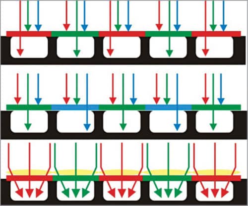
The space between adjacent light-sensitive pixels is used to house on-chip electronics. Micro lenses placed above the filter help in directing light into adjacent pixels. As outlined earlier, a single pixel allows photons of one colour only. Full-colour image is worked out by using a complex method called demosaicing. Simply stated, the camera treats each 2×2 set of pixels as a single unit, thereby providing one red, one blue and two green pixels. The actual colour is estimated based on the photon levels in each of these four pixels.
Electron multiplication CCD
Electron-multiplying CCD (EMCCD) technology helps to overcome the shortcoming of traditional CCD technology in offering high sensitivity at high speed. Traditional CCD sensors backed by readout noise figures of typically less than ten electrons offer high sensitivity. High sensitivity, however, comes at the cost of reduced speed of readout, which is typically less than 1MHz. The speed constraint arises from bandwidth limitation of the CCD charge amplifier. Increasing bandwidth, which is essential for high speed operation, increases noise too. That is, high-speed amplifiers are relatively noisier than their slow-speed counterparts.
Electron-multiplying CCD overcomes this limitation by building a unique electron multiplying structure into the chip. As a result, EMCCD as an image sensor is capable of detecting single photon events without an image intensifier. EMCCD sensors achieve high-sensitivity, high-speed operation by amplifying charge signal before the charge amplifier.
Most electron-multiplying CCDs utilise a frame-transfer CCD structure, wherein sensor area captures the image and storage area stores the image prior to readout. Storage area is normally identical in size to sensor area and is covered with an opaque mask, normally made of aluminium. When sensor area is exposed to light, an image is captured, which is automatically shifted downwards behind the masked region of the chip, and subsequently read out. During the readout process, another image is being captured by sensor area. The aluminium mask therefore acts like an electronic shutter.
As shown in Fig. 6, there is a multiplication register between the normal serial readout register and the charge amplifier. To read out the sensor, the charge is shifted out through the readout register and through the multiplication register where amplification occurs prior to readout by the charge amplifier.
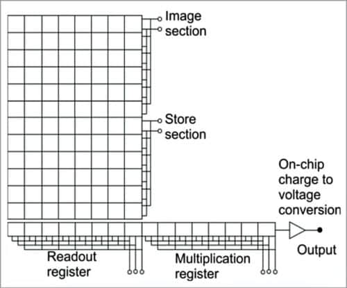
The multiplication register has several hundred stages or cells that use higher-than-normal clock voltages to achieve charge amplification. Amplification occurs in the multiplication register through a process known as clock-induced charge or spurious charge that occurs naturally in CCDs.
When clocking the charge through a register, there is a very small but finite probability (typically less than 2 per cent) that the charges being clocked can create additional charges by a process known as impact ionisation. Impact ionisation is the process by which a charge having sufficient energy creates another electron-hole pair. Hence a free electron charge in the conduction band can create another charge, leading to amplification.
Electron multiplication factor (M) may be computed from:
M=(1+p)N
where N is number of cells and p is the probability value. For instance, if the multiplication register had 512 cells or stages, and the probability of secondary electron generation were 1.3 per cent, the multiplication factor would be around 744. Electron multiplication prior to the output amplifier ensures that the readout noise introduced by the amplifier has negligible effect.
Major advantages of EMCCD sensors include high sensitivity in low light conditions, high-speed imaging capability, good daytime imaging performance and reduced likelihood of sensor damage while viewing in bright conditions. By elevating photon-generated charge above the readout noise of the device, even at high frame rates, the EMCCD meets the needs of ultra-low-light imaging applications without the use of external image intensifiers. The disadvantage is its relatively higher power consumption due to need for active cooling of the CCD.
The extreme low light capability of these EMCCDs enables a range of applications including border and coastal surveillance, surveillance of ports and airports, protection of sensitive sites and critical assets, and low-light scientific imaging such as in astronomy.
CMOS sensors
For their operation, both CCD and CMOS sensors depend on photoelectric effect to create electrical signal from light photons. These are two different technologies for digital image capture. Each has unique strengths and weaknesses for different applications.
In a CCD sensor, the quantum of charge held by different pixels is transferred through one or a very limited number of output nodes. Each pixel’s charge is converted into a proportional voltage and, after buffering, sent off-chip as an analogue signal. All of the pixels can be devoted to light capture and the output’s uniformity, which is a key factor in image quality, is high.
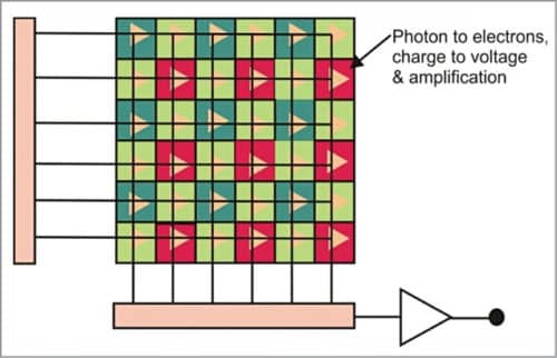
On the other hand, in a CMOS sensor, each pixel has its own charge-to-voltage convertor, amplifier and a pixel-select switch (Fig. 7). This is called active-pixel sensor architecture in contrast to passive-pixel sensor architecture used in a CCD sensor. Also, the sensor often includes on-chip amplifiers, noise-correction and analogue-to-digital conversion circuits, and other circuits critical to pixel sensors’ operation. The chip in this case outputs digital bits. Inclusion of these functions reduces the area available for light capture. Also, with each pixel doing its own conversion, uniformity and consequently image quality is lower. While readout mechanism of a CCD sensor is serial, it is massively parallel in the case of a CMOS sensor, allowing high total bandwidth for high speed.
CCD sensors versus CMOS sensors
Some of the key differences between CCD and CMOS sensors include:
1. Fabrication of CMOS sensors involves standard CMOS technology well established for fabrication of integrated circuits. This also allows easy integration of required electronics on the same chip, thereby resulting in devices that are compact and cost-effective. On the other hand, CCD sensor fabrication involves dedicated and costly manufacturing processes.
2. Compared to CCD sensors, CMOS sensors have relatively poor sensitivity and uniformity. The poor sensitivity is due to poor fill factor, while poor uniformity is due to the use of separate amplifiers for different pixels as against a single amplifier for all pixels in the case of CCD sensors.
3. CMOS sensors have higher speed than CCD devices due to the use of active pixels and inclusion of analogue-to-digital converters on the same chip leading to smaller propagation delays. Low-end CMOS sensors have low power requirements, but high-speed CMOS cameras typically require more power than CCD devices.
4. CCD sensors have higher dynamic range than CMOS sensors.
5. When it comes to temporal noise, CMOS sensors score over CCD sensors due to lower bandwidth of amplifiers at each pixel. But in terms of fixed-pattern noise performance, CCD sensors are better due to single-point charge-to-voltage conversion.
6. CMOS sensors allow on-chip incorporation of a range of functions such as automatic gain control, auto exposure control, image compression, colour encoding and motion tracking.
7. Due to the absence of shift registers, CMOS sensors are immune to smearing around over-exposed pixels, which is caused by spilling of charge into the shift register.
CCD sensors are used in cameras that offer excellent photo sensitivity and focus on high-quality, high-resolution images. CMOS sensors, on the other hand, are generally characterised by lower image quality, resolution and photo sensitivity. These are usually less expensive and have longer battery life due to lower power consumption. Also, these are fast achieving near parity with CCD devices in some applications.
Ladar sensors
Laser radars, also called Ladars, use a laser beam instead of microwaves. That is, in laser radars the transmitted electromagnetic energy lies in the optical spectrum, whereas in microwave radars it is in the microwave region. Frequencies associated with laser radars are very high, ranging from 30THz to 300THz. The corresponding wavelengths are 10µm to 1.0µm. Higher operating frequency means higher operating bandwidth, greater time or range resolution, and enhanced angular resolution. Another advantage of laser radars over microwave radars is their immunity to jamming.
Higher frequencies associated with laser radars permit detection of smaller objects. This is made possible by the fact that laser radar output wavelengths are much smaller than the smallest-sized practical objects. In other words, laser radar cross-section of a given object would be much larger than the microwave radar cross-section of the same. In fact, rain droplets and airborne aerosols too have significantly large laser-radar cross-section to allow their range and velocity measurement, which is very important for many meteorological applications. High resolution of laser radars allows recognition and identification of certain unique target features, such as target shape, size, velocity, spin and vibration—leading to their use for target imaging and tracking applications.
However, the performance of laser radars is affected by adverse weather conditions. Also, their narrow beamwidth is not conducive to surveillance applications. For surveillance applications, laser radars need to operate at very high repetition rates so that large volumes can be interrogated within the prescribed time. Alternatively, multiple simultaneous beams can be used.
Laser rangefinders are also a type of laser radars. A conventional laser rangefinder uses incoherent or direct detection. The term laser radar is usually associated with systems that use coherent detection.
Fig. 8 shows the block diagram of coherent laser radar. The laser beam is transmitted towards the target. A fraction of the transmitted power/energy reflected off the target is collected by the receiver. The laser radar in Fig. 8 is a monostatic system in which transmitter and receiver share common optics by using a transmit-to-receive switch. In bistatic arrangement, transmitting and receiving optics are separate. The received laser beam is coherently detected in an optical mixer.
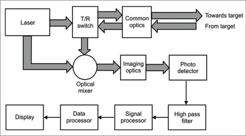
In the case of homodyne detection, a sample of transmitted laser power is used as local oscillator. In the case of heterodyne detection, another laser phase-locked to transmit laser is used as local oscillator. Heterodyne detection is used when transmitter and receiver are not colocated.
The output of the optical mixer is imaged onto the photo sensor. The electrical signal generated by the photosensor module is processed to extract the desired information about the target. The photosensor module is a single sensor in case of a scanning transmitted beam and a two-dimensional sensor array in case of a flash-type laser imaging radar.
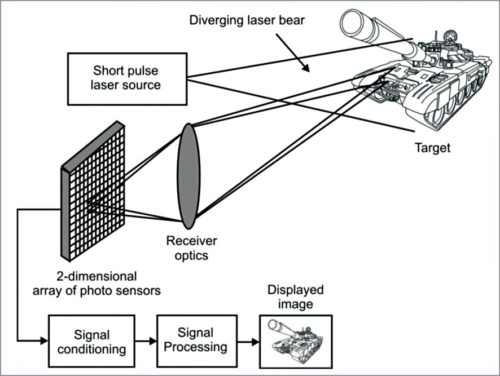
Fig. 9 illustrates the concept of flash-type 3D laser imaging. In this case, a diverging pulsed laser beam illuminates the entire scene of interest. The transmitted pulse time is referenced by an auxiliary photosensor. The back-scattered light is imaged onto a two-dimensional array of photosensing elements called pixels. While a conventional camera would measure the light intensity of back-scattered light pulse, in this case different sensor elements in the array measure time-of-flight. The time-of-flight is proportional to the distance between the point on the target from where the laser beam is reflected and the sensor element. The sensor array thus produces a 3D image of the target (angle-angle-range). An alternative approach of generating the target image is to use a scanning laser beam and a single sensor.
A common application of Ladar concept is in Ladar seekers, which are used mainly in conjunction with other guidance systems on strategic payloads for intended target discrimination from advanced decoys and aim-point selection. It is also well suited for combat identification, autonomous vehicle navigation and topography. Ladars are also suitable in finding targets hidden by camouflage nets and foliage.
Ladar seekers can detect and identify specific features of the target with very high definition, giving up to centimetre-level resolution from a few kilometres distance. An automatic target acquisition algorithm processes images to identify and acquire targets based on 3D templates stored in the weapon’s memory before the mission. Ladar sensors are usually employed on loitering systems that look at the target from different angles, verify target’s identity and select the best attack position for desired results.
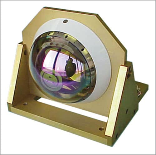
Fig. 10 shows an advanced multimode Ladar seeker from Lockheed Martin. The seeker can operate in standalone semi-active laser (SAL) and Ladar modes as well as simultaneous SAL and Ladar modes for target identification, acquisition and tracking. It is designed to conduct wide-area search and identify actual or potential targets including those obscured by camouflage or foliage.
Such Ladar seekers have been successfully tested on Loitering Attack Missile (LAM) missions under DARPA’s NLOS-LS (non-line-of-sight launch system) and USAF’s LOCAAS (Low-cost Autonomous Attack System) programmes. LAM with its multimode Ladar seeker searches a large area and relays location of various targets back to the command centre, where these targets are engaged by direct attack or other assets. In case of a priority target, LAM can be commanded to break off its search mission and attack the target.
To be continued…
Dr Anil Kumar Maini was formerly a scientist and director of Laser Science and Technology Centre (DRDO) and Nakul Maini is a postgraduate in optical engineering from University of Bristol (UK), currently working as analyst with Ericsson