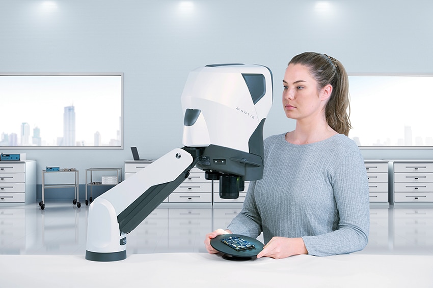
Here is the list of India’s Leading Suppliers and Manufacturers of Microscopes for Quality Control of Electronics.
List of Microscope Manufacturers and Suppliers in India
AMBITION TECHNOLOGIES
Website: www.ambitec.org
Address: 17-FF, Pocket 2, Sector 24, Rohini,
New Delhi – 110085 India
Email: [email protected]
Contact: 9810400671
Brand(s) Supplied: Ambition Technologies

BRUKER INDIA SCIENTIFIC PVT LTD
Website: www.bruker.com
Address: Unit Number 609, 6th floor, West Wing, Satellite Gazebo, Guru Hargovindji Marg, Andheri Ghatkopar Road, Andheri (East), Mumbai-400093
Email: [email protected]
Contact: 022 6112 8809
Brand(s) Supplied: Bruker
Indian OEMs
| Company | Website | City |
| Ambition Technologies | https://www.ambitec.org | Delhi |
| Cosmo Laboratory Equipment | www.coslabindia.com | Ambala Cantt |
| Dynascan Inspection Systems Company | www.dynascan.info | Bengaluru |
| ESAW India | esawindia.com | Ambala Cantt |
| ESC Medicams | https://www.escmedicams.com/pcb- inspection-camera | Delhi |
| Focus Nano Technology | www.focusnanotechnology.com | Bengaluru |
| Gaby Instruments | https://www.gabyinstruments.in | Coimbatore |
| Getner Instruments Pvt Ltd | https://getnermicroscopes.com/know-us | Ambala Cantt |
| Imtronics Technology | https://imtronics.in/pick-and-place-machine | Noida |
| JB Instruments Pvt Ltd | www.jbinstruments.com | New Delhi |
| Labomed India Pvt | www.labomedworld.com | Gurugram |
| Magnus opto systems | https://www.magnusopto.com | New Delhi |
| Matrix Testing Machine Services | matrixmachines.net | Pune |
| Nuline Technologies | https://nulineindia.com/products/nulinescope | Bengaluru |
| Quality Scientific & Mechanical Works (Quasmo) | https://www.quasmoindianmicroscope.com | Ambala |
| Radical Scientific Equipments Pvt | https://www.radicalindia.com | Ambala Cantt |
| Vision Microsystems | https://www.visionmicroscope.com | Kolkata |
COLE-PARMER INDIA
Website: www.coleparmer.in
Address: 403, A-Wing Delphi, Hiranandani Business Park, Mumbai 400076, India
Email: [email protected]
Contact: 022-61394444
Brand(s) Supplied: Cole Parmer, Motic, Meiji Techno
COSMO LABORATORY EQUIPMENT
Website: www.coslabindia.com
Address: 3474, Shantipath, Ram Bagh Road, Ambala Cantt, Haryana- 133001
Email: [email protected]; [email protected]
Contact: 9416113230
Brand(s) Supplied: Cosmo Laboratory
DAIICHI JITSUGYO INDIA PVT LTD
Website: djkindia.co.in
Address: Ground Floor, Time Tower, 002, Mehrauli-Gurgaon Road, Gurugram, Haryana -122002
Email: [email protected]
Contact: 9319518112
Brand(s) Supplied: Vision Engineering
DYNASCAN INSPECTION SYSTEMS COMPANY
Website: www.dynascan.info
Address: No. 39- P/1, Phase- 2 (East), Electronic City, Hosur Road, Bengaluru – 560100, India.
Email: [email protected]
Contact: 9741109039
Brand(s) Supplied: Dynascan Inspection
ELEMENT14 INDIA PRIVATE LIMITED
Website: in.element14.com
Address: D Block, 11th Floor, IBC Knowledge Park, 4/1, Bannerghatta Main Rd, Bhavani Nagar, Suddagunte Palya, Bengaluru, Karnataka 560029
Email: [email protected]
Contact: 1800 108 3888
Brand(s) Supplied: Kern, Miller, Aven Tools,
Cif, Vision Engineering & Ideal-tek
Global OEMs In India
| Bruker India Scientific Pvt Ltd Website: www.bruker.com City: Mumbai Evident Scientific Pvt Ltd Website: evidentscientific.com City: Gurugram Hitachi High-Tech India Pvt Ltd Website: www.hitachi-hightech.com City: Gurugram KEYENCE INDIA PVT LTD Website: www.keyence.co.in City: Chennai Leica Microsystems Website: www.leica-microsystems.com City: Mumbai Thermo Fisher Scientific India Pvt Ltd Website: https://www.thermofisher.com City: Mumbai Vision Engineering Ltd (VE Quality Instrumentation) Website: https://www.visioneng.com City: Mumbai Zeiss Group Website: https://www.zeiss.com City: Bengaluru |
ESAW INDIA
Website: esawindia.com
Address: 527, P.P.P, Near HSIDC Industrial Park, Ambala Cantt, Haryana 133006
Email: [email protected]
Contact: 9335555599
Brand(s) Supplied: ESAW
ESC MEDICAMS
Website: www.escmedicams.com/pcb-inspection-camera
Address: 157, Old Lajpat Rai Market, Chandni Chowk, New Delhi – 110006
Email: [email protected]
Contact: 9818100144
Brand(s) Supplied: ESC Medicams
EVIDENT SCIENTIFIC PRIVATE LIMITED
Website: evidentscientific.com
Address: 201-203, Tower C, Unitech Cyber Park, Sector – 39, Gurugram-122002
Email: [email protected]
Contact: 0124 6942800
Brand(s) Supplied: Evident Scientific
10 Leading Global Brands
These companies are widely recognised for their innovations, quality, and global presence.
| company | website | HQ City/Country |
| AmScope (United Scope LLC) | www.amscope.com | Irvine, California, USA |
| Andonstar | www.andonstar.com | Shenzhen, China |
| Hirox Co., Ltd | www.hirox.com | Tokyo, Japan |
| JEOL Ltd | www.jeol.com | Tokyo, Japan |
| Leica Microsystems | www.leica-microsystems.com | Wetzlar, Germany |
| Nikon Instruments | www.microscope.healthcare.nikon.com | Tokyo, Japan |
| Olympus (now Evident Corporation) | www.olympus-lifescience.com | Tokyo, Japan |
| TESCAN Orsay Holding | www.tescan.com | Brno, Czech Republic |
| Vision Engineering | www.visioneng.com | Send Woking, UK |
| Zeiss (Carl Zeiss AG) | www.zeiss.com | Oberkochen, Germany |
FOCUS NANO TECHNOLOGY
Website: www.focusnanotechnology.com
Address: No. 467, 2nd Floor, RTBI Campus, Peenya Industrial Area, Phase IV, Bangalore North, Bengaluru, Karnataka – 560058
Email: [email protected]
Contact: 9886445830
Brand(s) Supplied: Focus Nano Technology
GABY INSTRUMENTS
Website: www.gabyinstruments.in/
Address: 4/231, lions Garden, Appanaickan Patti, Sulur tk, Coimbatore, india
Email: [email protected]; [email protected]
Contact: 8220496222
Brand(s) Supplied: Gaby Instruments

GETNER INSTRUMENTS PVT LTD
Website: getnermicroscopes.com/know-us/
Address: #121, HSIIDC Industrial Estate, Jagadhari Road, Ambala Cantt-133006
Email: [email protected]; [email protected]
Contact: 0171-2699120
Brand(s) Supplied: Getner
HITACHI HIGH-TECH INDIA PVT LTD
Website: www.hitachi-hightech.com
Address: Unit No 706, Part-A, 7th Floor, Tower D, Unitech Cyber Park, Sector 39, Gurugram 122002
Email: [email protected]
Contact: 0124 4417709
Brand(s) Supplied: Hitachi-hightech
IMTRONICS Technology
Website: imtronics.in/pick-and-place-machine/
Address: G-312, Ground Floor, Sector-63, Noida – 201301
Email: [email protected]
Contact: 0120-4268884
Brand(s) Supplied: Imtronics
JB INSTRUMENTS PRIVATE LIMITED
Website: www.jbmicroscope.com
Address: J-9/36, UNIT NO:- 402 & 403, 2nd Floor, Rajouri Garden, New Delhi-110027
Email: [email protected]
Contact: 9873571533
Brand(s) Supplied: JB Microscope
KAMPFER AUTOMATION PRIVATE LIMITED
Website: www.kampferindia.com
Address: 119, E-20, BDA, Domlur 2nd Stage,
Bengaluru, Karnataka -560071
Email: [email protected]
Phone: 080-25351440
Brand(s) Supplied: Tagarno
| When to Use What |
| • Routine Production/Rework → Stereo or Digital Microscope • Defect Localisation/Fine Features → Compound or Metallurgical Microscope • Stress/Crystalline Material Studies → Polarising Microscope • Mounted/Large Samples → Inverted Microscope • Advanced Failure Analysis/Nano-scale Inspection → SEM |
KEYENCE INDIA PVT LTD
Website: www.keyence.co.in
Address: Olympia Cyberspace, 10th Floor-Office No-1, No.21/22, Alandur Road, Guindy, Chennai – 600032, Tamil Nadu
Email: [email protected]
Contact: 1-800-103-0090
Brand(s) Supplied: Keyence
KONTRELEK INSTRUMENTS
Website: dinolite-india.co.in/
Address: 44, Electronic Estate, Off Pune – Satara Road, Pune 411009
Email: [email protected]
Contact: 9049997269
Brand(s) Supplied: Dino-lite
LAB INDIA INSTRUMENTS
Website: www.labindiainstruments.com
Address: 201, Nand Chambers, L B S Marg, Near Vandana Cinema, Thane – 400602
Email: [email protected]
Contact: 022 69086000
Brand(s) Supplied: Nikon
Features To Look While Selection
| Feature | Why It Is Important | What To Look For |
| Magnification Power | The core of PCB inspection lies in the ability to clearly visualise fine details like solder joints, micro-traces, and potential defects. Most standard inspections require magnification in the range of 10x to 100x, while high-density or multilayer PCBs may demand up to 500x-1000x for inspecting micro-components or BGA (Ball Grid Array) connections. | • Optical zoom vs digital zoom (optical preferred for clarity) • Zoom range adjustability (smooth, click-less control preferred) • Crisp edge-to-edge clarity without spherical or chromatic distortion |
| Working Distance | Working distance refers to the space between the microscope’s objective lens and the PCB. A longer working distance allows ample room for soldering, rework, or probe testing without disturbing the focus. | • 70mm to 100mm is considered optimal for electronics inspection and hands-on work |
| Lighting | Clear visibility is essential to identify hairline cracks, poor solder joints, or oxidation. LED ring lights and oblique-angle lighting help reduce reflections from metallic surfaces and enhance contrast. | • Adjustable LED intensity (with dimmers) • Coaxial or side lighting for depth inspection • Polarised light filters to reduce glare • Choose microscopes with dual-lighting systems (top and bottom) for both opaque and translucent PCBs |
| Ergonomics | An ergonomically designed microscope reduces fatigue and eye strain, leading to faster and more accurate inspections. | • Eyepiece free design offering freedom of head movement and use of spectacles • Tiltable viewing heads or trinocular tubes • Adjustable height stands • Anti-fatigue posture design for prolonged sessions |
| Digital Connectivity | Modern digital microscopes streamline documentation, remote collaboration, and quality control. USB or HDMI output allows real-time display on monitors, and onboard cameras support high-resolution image and video capture. | • 1080p or 4K HDMI camera output • USB-C or USB 3.0 connectivity • Built-in software for image annotation and measurement • Wi-Fi/Cloud integration (for advanced collaborative workflows) |
Types of Microscopes
| Type | Description | Key Applications in Electronics | Magnification Range (Typical) | Advantages | Limitations |
| Stereo Microscope | Uses two optical paths for 3D visualisation with a wide field of view | Inspecting PCBs, solder joints, wire bonding, and component alignment during assembly and rework | 5x–80x | • 3D depth perception for soldering/rework • Easy to use, wide field view • Compatible with ESD-safe benches | • Limited magnification • Not suitable for nano-scale inspection |
| Compound Microscope | High-magnification light microscope with multiple objective lenses for 2D imaging | Examining fine circuit traces, contamination, and micro-cracks in semiconductors | 40x–1000x | • High resolution imaging • Good for fine details in thin films and defects | • Flat 2D view (no depth) • Requires thin/transparent samples |
| Inverted Microscope | Views sample from below; suitable for larger/mounted specimens | Inspecting encapsulated PCBs, coated wafers, or layered semiconductor processes | 40x–400x | • Can handle bulky/mounted samples • Useful for live processes or coated layers | • Moderate magnification • Bulkier and costlier than stereo microscopes |
| Metallurgical Microscope | Uses reflected light for opaque/metallic surfaces | Inspecting metal interconnects, solder balls, welds, wafers for cracks or impurities | 50x–500x | • Excellent for opaque and reflective surfaces • Identifies cracks, voids, inclusions in metals | • Limited to surface inspection • Less effective for transparent samples |
| Polarising Microscope | Uses polarised light to enhance contrast in birefringent materials | Studying stress patterns, crystalline defects, thin film alignment | 10x–400x | • Highlights stress and crystalline structures • Useful for materials R&D | • Niche application • Requires specialised training |
| Digital Microscope | Integrates optics, camera, and display; may include software for measurement and reporting | Documentation, training, defect reporting, and high-volume inspections in production lines | 20x–500x (variable zoom) | • Easy sharing and recording • Software-enabled measurement • Useful for remote collaboration | • Lower optical quality than dedicated optical scopes • May have lag or resolution limits |
| Scanning Electron Microscope (SEM) | Uses electron beams for ultra-high-resolution (nano-scale) imaging | Failure analysis, nano-defect detection, material studies, wafer surface morphology | Up to 100,000x+ | • Extremely high resolution • Enables material composition analysis (with EDS add-on) • Critical for advanced semiconductor R&D | • Very expensive • Requires vacuum and skilled operators • Slow compared to optical scopes |
| Atomic Force Microscope (AFM) | Uses a sharp probe to scan the surface at the atomic level, measuring forces between the tip and sample | Nano-scale surface characterisation, thin film measurement, defect detection in semiconductors, and 3D surface profiling | Up to ~1,000,000x (atomic resolution) | • Provides true 3D topographic images • Can measure mechanical, electrical, and magnetic properties at nano-scale • Works in air, vacuum, or liquid environments | • Very slow scan speed • Limited scan area • Delicate probes and high operator skill required • Very high cost |
LABOMED INDIA PVT
Website: www.labomedworld.com
Address: 903, 9th Floor, Time Tower, M.G. Road, Gurugram India
Email: [email protected]
Contact: 8882792899
Brand(s) Supplied: Labomed
LEICA MICROSYSTEMS
Website: www.leica-microsystems.com
Address: 3rd Floor B Wing Art Guild House Phoenix Market City LBS Road, Kurla West, Mumbai, 400070 India
Email: [email protected]
Contact: 7290075040
Brand(s) Supplied: Leica
MAGNUS OPTO SYSTEMS
Website: www.magnusopto.com
Address: A-5, Mohan Co-operative Industrial Estate, New Delhi-110044, India
Email: [email protected]
Contact: 9717710061
Brand(s) Supplied: Magnus opto systems
| Key IPC Standards |
| IPC standards ensure visual inspections meet quality benchmarks, with microscope usage tied to magnification and resolution requirements. Key standards include: • IPC-A-610 (Acceptability of Electronic Assemblies): Defines visual criteria for assemblies, requiring magnification aids (e.g., 1.75x–4x for general inspection, up to 10x for fine details). It influences microscope selection—digital systems for documentation, binocular for precise work—and mandates lighting and training. • IPC-J-STD-001 (Requirements for Soldered Electrical and Electronic Assemblies): Specifies inspection methods, including microscope use for solder joint evaluation • IPC-A-600 (Acceptability of Printed Boards): Focuses on PCB appearance and structure, recommending microscopes for internal inspections. • IPC-TM-650 (Test Methods Manual): Provides guidelines for evaluating PCBs, including visual methods under magnification. • IPC-OI-645 (Optical Inspection Guidelines): Defines requirements for optical inspection of electronic assemblies, covering magnification ranges, resolution, lighting, and calibration. It guides the use of binocular, digital, or AOI systems for consistent defect detection and stresses operator training for reliable inspection results. For full IPC standards, visit ipc.org |
MATRIX TESTING MACHINE SERVICES
Website: matrixmachines.net
Address: Office No. 813, 8th Floor, Rama Equator, Near Finolex Chowk, Pimpri, Pune – 411018, Maharashtra, India
Email: [email protected]
Contact: 72760 01181/91122 11910
Brand(s) Supplied: Matrix Testing Machine Services
MAXIM SMT
Website: www.maximsmt.com
Address: Plot No.78 A, Sector-5, IMT Manesar, Gurugram-122050, Haryana
Email: [email protected]
Contact: 0124 4354974-75
Brand(s) Supplied: Zenzon
NANOTECH TMI
Website: nanotech-tmi.com
Address: Unit No. 1024, Tower A, Spaze IT Park Sector, 49, Sohna Road, Gurugram 122018, Haryana, India
Email: [email protected]
Contact: 70428 14134
Brand(s) Supplied: Nikon
NECTOR EMS TECHNOLOGIES
Website: www.nectorems.com/
Address: Street No-09, Gali Number 9, Block A, Dabri Extension East, Dabri, New Delhi, Delhi, 110045
Email: [email protected]
Contact: 9315560437
Brand(s) Supplied: Heroj
NMTRONICS INDIA PVT. LTD.
Website: www.nmtronics.com
Address: SDF NO. E-17 & C-2, Noida Special Economic Zone Noida Dadri Road, Phase-II, Noida- 201305
Email: [email protected]
Contact: 0120 4603500
Brand(s) Supplied: Vision Engineering
Technology Advancement In Microscopes
| Technology Advancement | Benefit / What It Solves | Electronics Industry Use Case / Scenario |
| 4K Ultra-HD Digital Imaging | Reveals micro-cracks, voids, solder bridges in fine-pitch components | BGA, QFP, microvia inspection, Class 3 PCB |
| Multi-Angle / Ring Lighting with Shadow Enhancement | Highlights hidden or low-contrast surface defects | Inspection of solder joints, pin misalignments, bottom-terminated devices |
| AI-Assisted Solder Joint & Component Inspection Apps | Automates defect detection and pass/fail tagging | Automated visual QA on SMT line, repair analysis |
| Real-Time 3D Profiling / Focus Stacking | Depth-corrected full-focus images across uneven PCB surfaces | Uneven solder, lifted pads, BGA rework zone analysis |
| Auto Image Comparison with Golden Board Reference | Detects even the smallest process drift or missing parts | Inline QA, batch verification, IPC inspection audits |
| Integrated 2D/3D Measurement Tools | Measures land width, solder height, component alignment | IPC-A-610 Class 2/3 compliance, production reporting |
| Elemental Analysis Add-On (XRF Integration) | Identifies solder alloy, plating material, contamination | Failure root cause analysis, corrosion tracking |
| Ergonomic Eyepiece-Free 3D Viewing | Reduces operator eye fatigue, improves productivity | Manual inspection and repair stations |
| Automated Report Generation & Traceability | Streamlines documentation for quality audits | Class 3 QA reporting, MES integration, remote audits |
| Live Remote Streaming / Multi-user View | Enables remote inspection, customer collaboration | OEM vendor audits, offshore quality assurance |
NULINE TECHNOLOGIES
Website: nulineindia.com/products/nulinescope
Address: 2711, 2 Main, HAL 3 Stage, Bengaluru – 560 075, Karnataka, India
Email: [email protected]
Contact: 080 25287888
Brand(s) Supplied: Nuline
PCI AUTOTRONICS PVT LTD
Website: pciautotronics.com/index.php/electronics
Address: 287-288 Udyog Vihar, Phase II, Gurugram, Haryana-122016
Email: [email protected]
Contact: 0124 6656999
Brand(s) Supplied: Caltex Scientific
QUALITY SCIENTIFIC & MECHANICAL WORKS (QUASMO)
Website: www.quasmoindianmicroscope.com
Address: #84 HSIIDC, Industrial Estate, Ambala-133001
Email: [email protected]
Contact: 8926666632
Brand(s) Supplied: Quasmo
RADICAL SCIENTIFIC EQUIPMENTS PVT
Website: www.radicalindia.com
Address: 9th Mile Stone, Ambala-Jagadhri Road, NH-444A, Ambala Cantt-133104
Email: [email protected], [email protected]
Contact: 171-2977793
Brand(s) Supplied: Radical Scientific Equipments Pvt.
SUMITRON EXPORTS PVT LTD
Website: sumitron.com/products
Address: No. F19/1, Sector 8, Rohini, Near M2K Cinema Hall, Delhi – 110085
Email: [email protected]
Contact: 011 43824444
Brand(s) Supplied: Vitiny
TANOTIS PRIVATE LIMITED
Website: www.tanotis.com/
Address: 1st Floor, Site No. 1, SFHS, Nandini Layout, Bengaluru, Karnataka – 560096
Email: [email protected]
Contact: 9686002002
Brand(s) Supplied: Celestron, Konus, National Optical, Dura Tool, Carson, Barska
THERMO FISHER SCIENTIFIC INDIA PVT. LTD.
Website: www.thermofisher.com
Address: 403-404, Delphi “B” Wing, Hiranandani Business Park, Powai, Mumbai – 400076
Email: [email protected]
Contact: 022-66803000
Brand(s) Supplied: Thermofisher
VISION ENGINEERING LTD (VE QUALITY INSTRUMENTATION)
Website: www.visioneng.com
Address: B‑803 Sagar Tech Plaza, Andheri Kurla Road, Sakinaka, Mumbai, Maharashtra, 400072
Email: [email protected]
Contact: 022 49726600
Brand(s) Supplied: Vision Engineering
VISION MICROSYSTEMS
Website: www.visionmicroscope.com/
Address: UNIT: 118, 1st Floor, CITY MALL, AIRPORT CITY-II, Airport Gate No. 3, Dum Dum, Kolkata – 700081, West Bengal, India
Email: [email protected]
Contact: 9433867042
Brand(s) Supplied: Vision Microsystems
ZEISS GROUP
Website: www.zeiss.com
Address: Plot No. 3, Jigani Link Road, Bommasandra Industrial Area, Bengaluru- 560099
Email: [email protected]
Contact: 080 43438102
Brand(s) Supplied: Zeiss

We published the list of manufacturers and suppliers of pick-and-place machines and selective soldering systems.