
A new 3D nanoscale imaging method now reveals how different passivation strategies reshape internal charge pathways offering a clearer roadmap for boosting performance and accelerating commercial deployment.
Researchers in China have developed a three-dimensional electrical imaging method that for the first time visualizes how defect passivation treatments influence charge transport inside perovskite solar films, a breakthrough that could accelerate commercial adoption of perovskite photovoltaics by linking nanoscale behavior to cell performance.
Perovskite solar cells are among the most promising next-generation photovoltaic technologies due to their high efficiency and low manufacturing cost compared with silicon. But persistent defects inside perovskite films have limited charge transport, reducing energy output and long-term stability are key hurdles for industrial deployment.
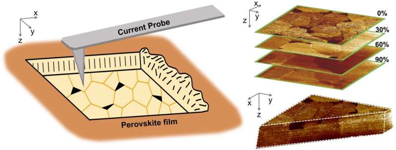
At the Ningbo Institute of Materials Technology and Engineering, part of the Chinese Academy of Sciences (CAS), scientists tackled this challenge by advancing tomographic conductive atomic force microscopy (TC-AFM), enabling nanoscale 3D electrical mapping of perovskite films. Traditional characterization methods typically probe only surface layers or average properties, obscuring how treatments affect deeper regions of the material.
The new technique works by sequentially shaving ultrathin slices from the film while measuring local electrical conductivity at each depth, reconstructing a full 3D profile of current pathways. This high-resolution view revealed how different passivation strategies alter internal electrical behavior in ways previously inferred only indirectly.

In untreated films, extensive low-conductivity zones especially at grain boundaries were shown to block charge carriers. Bulk passivation significantly reduced these dead zones throughout the interior, while surface passivation mainly improved conductivity near the top interface, important for integrating the film into full devices. The most uniform conductive networks emerged in films that combined both treatments.
Crucially, the 3D electrical signatures correlated strongly with overall solar cell efficiency, establishing a direct mechanistic link between passivation chemistry and performance outcomes. According to lead researchers, this connection could guide rational optimization of passivation treatments, cutting trial-and-error in materials design and helping close the gap toward stable, high-efficiency perovskite commercial modules. The approach also holds potential beyond photovoltaics offering a tool for probing internal charge dynamics in a broad class of thin-film electronic and optoelectronic materials.