


Roadmap outlines how two-dimensional indium selenide could address silicon’s scaling and power limitations, detailing its electronic properties, device potential, and the manufacturing challenges that must be overcome for integration into next-generation low-power computing systems.
A new research roadmap by Sungkyunkwan University positions two-dimensional indium selenide (InSe) as a potential successor to silicon in ultra-scaled electronics, outlining both its device-level advantages and the manufacturing barriers that must be solved before commercial adoption.
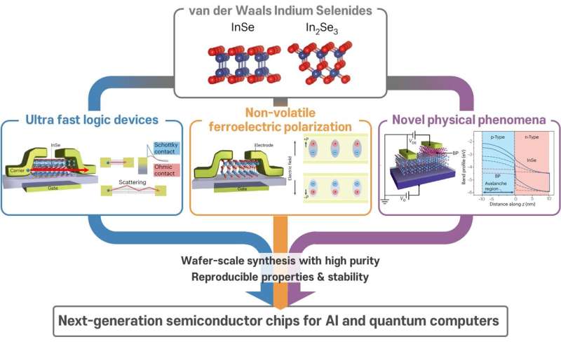
As silicon transistors approach atomic-scale dimensions, engineers are confronting rising leakage currents, heat density, and diminishing performance gains. The latest roadmap, published in Nature Reviews Electrical Engineering and reported by Tech Xplore, evaluates whether InSe — a layered quantum semiconductor — can extend Moore’s Law–style progress without the same energy penalties.
At the material level, InSe offers high electron mobility and near-ballistic transport, allowing charge carriers to move with minimal scattering. Researchers argue that this property could enable faster switching at lower voltages than conventional silicon channels. The material’s low effective electron mass is also seen as a factor in reducing power consumption in highly scaled devices.
Beyond conventional transistor behavior, InSe exhibits ferroelectric characteristics, meaning it can maintain polarization states without continuous power. This opens the possibility of integrating logic and memory functions within a single material platform — a shift that could reduce data-transfer bottlenecks that dominate today’s AI and high-performance computing architectures.
The roadmap also addresses integration challenges. Producing wafer-scale, defect-free InSe layers remains difficult, particularly given the material’s sensitivity to oxidation. Researchers outline encapsulation strategies, contact engineering approaches, and fabrication process adjustments needed to align InSe devices with existing CMOS infrastructure.
While silicon is unlikely to disappear from mainstream manufacturing in the near term, the study frames InSe as part of a broader post-silicon strategy. If materials engineering and large-scale processing challenges can be resolved, InSe-based devices could find roles in ultra-low-power processors, embedded memory, and potentially quantum-adjacent electronics. The roadmap signals that next-generation semiconductor progress may depend less on shrinking silicon and more on rethinking the material foundation of electronic circuits.