


New semiconductor design unlocks faster, denser, and more reliable NAND storage for future electronics
An advancement in semiconductor design could significantly expand data storage capacity while improving speed and reliability, addressing one of the biggest bottlenecks in modern electronicsfrom smartphones to AI data centres.
Researchers at the Korea Advanced Institute of Science and Technology (KAIST) have developed a “smart gate” architecture that enables more efficient control of electron movement in NAND flash memory. The innovation targets the scaling limits of 3D V-NAND, a widely used storage technology that is increasingly struggling to pack more data into smaller physical footprints.
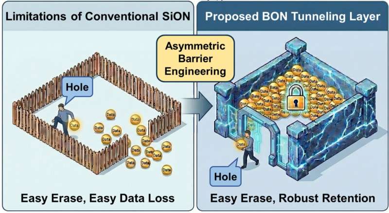
At the core of the advancement is a new tunnelling layer materialboron oxynitride (BON), which replaces conventional silicon-based materials. Unlike traditional approaches, this material creates an asymmetric energy barrier, enabling the semiconductor to selectively regulate electron flow under varying operating conditions. This helps resolve a long-standing trade-off between speed and data retention reliability in memory devices.
The impact is particularly relevant to next-generation penta-level cell (PLC) memory, which stores 5 bits per cell by distinguishing among multiple voltage states. While PLC promises significantly higher density, it has been limited by performance degradation and instability. The smart gate structure addresses these issues, enabling faster write and erase operations without increasing leakage.
Beyond performance gains, the development comes at a critical time for the semiconductor industry. Demand for high-density memory is surging due to AI workloads and data-intensive applications, while existing scaling techniques are approaching physical and material limits. By overcoming these constraints, the smart gate approach could serve as a key enabler for ultra-high-capacity storage in future electronic systems. The technology was presented at the IEEE International Electron Devices Meeting (IEDM), highlighting its potential relevance for both academic research and commercial semiconductor roadmaps.
If successfully commercialised, this innovation could reshape memory architectures, allowing manufacturers to deliver higher-capacity chips without significantly increasing size, an essential step for advancing AI infrastructure, edge devices, and next-generation consumer electronics.