


A surprising ultrathin material is challenging long-standing limits in chip fabrication, hinting at a new way to shape nanoscale circuits with greater precision and resilience.
An international team of researchers led by Saptarshi Das, Ackley Professor at Pennsylvania State University, has reported a new approach to semiconductor patterning using an atomically thin material, chromium oxychloride (CrOCl), in a study published in Nature Materials. The work focuses on improving the hard mask layer used during chip fabrication, a key step that defines nanoscale circuit features.

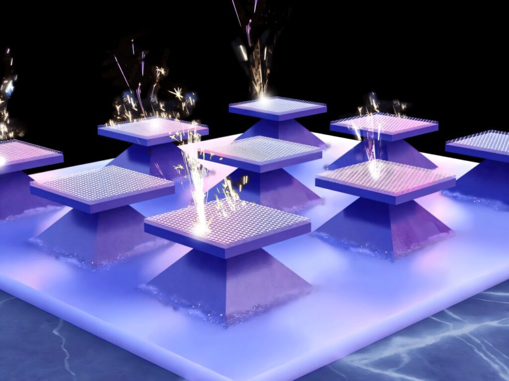
Patterning is central to modern semiconductor manufacturing, where intricate structures are etched into materials to form circuits found in devices ranging from sensors to computing systems. This process relies on hard masks, thin protective layers that shield selected regions while exposed areas are removed through plasma etching. However, as device dimensions shrink and architectures become more complex, conventional mask materials struggle to withstand the harsh chemical environments involved.
Current industry-standard materials, including silicon dioxide and metal-based compounds, gradually degrade under plasma exposure, limiting precision and reliability. The researchers explored two-dimensional metal oxyhalides, identifying chromium oxychloride as a promising alternative. The material’s layered crystal structure plays a critical role. Weak bonding between layers allows the surface to form a passivation layer under plasma exposure, which becomes chemically inert and protects the underlying material.
The study also found that chromium oxychloride surface smooths out, rather than becoming rougher, reducing defects associated with uneven etching. This effect helps prevent micro-masking, a common issue where redeposited byproducts interfere with pattern formation. As a result, the material enables sharper and more vertically defined features, which are essential for advanced three-dimensional chip integration.
Another aspect of the material is its ability to be patterned separately and then transferred onto different substrates, including flexible materials. This could expand fabrication options beyond rigid silicon platforms. While the findings highlight potential advantages, the research remains at an early stage. Demonstrations have been limited to small samples, and further work is required to scale the material for wafer-level manufacturing.
