Rice researchers develop near-perfect 2D perovskite crystals enabling record energy transport, boosting performance for solar cells and optoelectronics while overcoming structural limits in hybrid semiconductor materials.
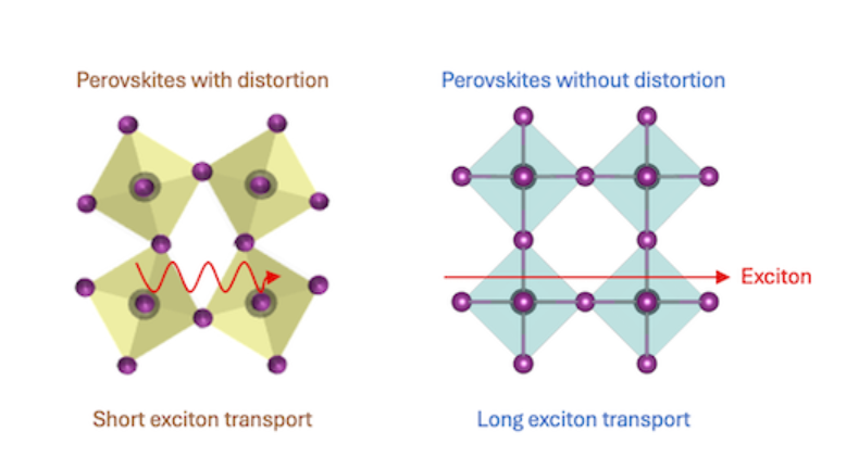
Researchers have engineered a near-perfect two-dimensional semiconductor that significantly improves energy transport, marking a key advance for next-generation optoelectronic devices. The work focuses on 2D metal halide perovskites—hybrid materials widely studied for solar cells and light-emitting devices, but historically limited by structural distortions that trap energy. By eliminating these distortions, the team created a multilayered crystal with near-ideal symmetry, enabling energy to move freely through the material.

At the core of the advancement is crystal symmetry. Conventional perovskites tend to form soft, irregular lattices, disrupting charge transport. The new structure maintains uniformity across layers, allowing excitons—energy-carrying quasiparticles formed from absorbed light—to travel more than two micrometres without loss, a performance rarely seen in such materials.
This represents an order-of-magnitude improvement over previous 2D perovskites and brings performance in line with advanced materials such as transition-metal dichalcogenides, which are used in high-end sensors and integrated electronics. The researchers achieved this by altering the fabrication process. Instead of allowing crystals to fully settle at lower temperatures—where distortions typically emerge—they stabilised the structure earlier, preserving symmetry. The approach also enabled thicker, multilayered configurations, overcoming prior limits that allowed only thinner forms to be reliably produced.

The implications extend across semiconductor applications. Improved exciton transport can directly enhance efficiency in solar cells, photodetectors and light-emitting devices, where energy losses currently constrain performance. The material’s stability and near-ideal band gap further position it for integration with silicon in tandem solar architectures. While still in the research stage, the findings demonstrate how precise control at the atomic level can unlock significant gains in energy transport. For the electronics industry, this could translate into more efficient, scalable components for next-generation energy and computing systems.