


Researchers at Pohang University of Science and Technology have tackled a major bottleneck in electronics for ultra-thin semiconductors, cutting contact resistance by 50-fold and dramatically improving transistor performance for future 3D chip architectures.
As the semiconductor industry pushes toward ever-thinner transistors, researchers have found a way to overcome a long-standing performance barrier that has limited the practical use of ultra-thin electronic devices. A team from the South Korean POSTECH research institute has developed a localised thick-contact design that significantly improves current flow in ultra-thin tellurium transistors, a promising technology for next-generation chips.
The breakthrough addresses a fundamental challenge in advanced semiconductor scaling. While shrinking transistor channels below 5 nanometers helps reduce leakage current and improve efficiency, it also increases the resistance at the metal-semiconductor interfaces. This resistance, known as contact resistance, restricts electron flow and reduces overall device performance.
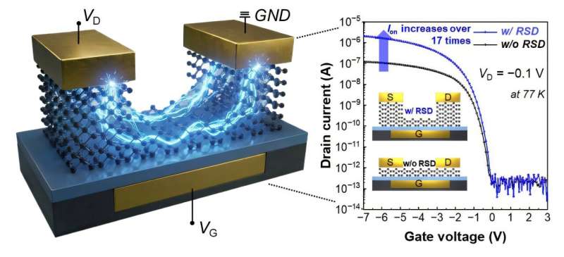
To solve the problem, the researchers adopted a selective thickening strategy. Instead of increasing the thickness of the entire transistor, they deposited additional tellurium only in the source and drain regions where electrical contacts are formed. The transistor channel itself remained ultra-thin at 4 nanometers, preserving low leakage characteristics while improving conductivity at critical junctions.
Testing showed substantial gains. The redesigned structure reduced contact resistance from 97.5 kΩ·μm to 1.7 kΩ·μm, representing a 50-fold improvement. At low temperatures down to -196°C, the transistors delivered more than 17 times higher on-state current than conventional ultra-thin designs.
The advance arrives as chipmakers increasingly explore three-dimensional semiconductor architectures that stack logic and memory vertically to improve computing efficiency. Such designs are viewed as a key path beyond traditional transistor scaling, especially as artificial intelligence and high-performance computing workloads drive demand for faster data movement and lower power consumption.
Equally important for the electronics industry, the new approach is compatible with low-temperature sputtering processes and large-area manufacturing techniques, making it suitable for future mass production. Researchers believe the localised thickness-control method could be extended beyond tellurium to a wider range of ultra-thin and two-dimensional semiconductor materials used in advanced electronic systems.