


MIT researchers have developed electronic-photonic integration technologies that could enable petabit-scale data transfer while reducing power consumption, paving the way for more efficient semiconductor packaging and next-generation data centre infrastructure.
The push for faster, more energy-efficient semiconductor systems has taken a significant step forward as researchers at MIT unveiled new electronic-photonic integration technologies capable of dramatically increasing data bandwidth while reducing power consumption. The advances are designed to overcome one of the biggest challenges in modern chip design—efficiently transferring massive amounts of data without escalating energy demands.
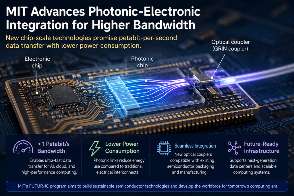
Developed under the FUTUR-IC research program, the new microsystem architecture combines traditional electronic circuits with photonic components that transmit information via light rather than electrical signals. By leveraging photonics for communication and electronics for computation, the platform aims to deliver data transmission speeds exceeding 1 petabit per second, a substantial leap from today’s systems operating in the hundreds of terabit-per-second range.
A key innovation is the introduction of new optical coupling devices that simplify the integration of photonic chips with conventional semiconductor packages. Among them are the graded index (GRIN) coupler and the previously demonstrated evanescent coupler, both engineered to reduce the complexity and cost of connecting optical and electronic components within the same package. Importantly, these devices are compatible with existing semiconductor foundries and packaging infrastructure, avoiding the need for entirely new manufacturing processes.
The technology addresses a growing concern across the electronics industry as AI workloads, cloud computing, and hyperscale data centres continue driving demand for higher bandwidth. Conventional electrical interconnects consume increasing amounts of energy as data rates rise, whereas optical communication offers significantly better energy efficiency. Researchers believe hybrid electronic-photonic systems could help contain the soaring electricity consumption of future computing infrastructure while supporting higher-performance processors.
Beyond hardware innovation, the FUTUR-IC initiative is also investing in workforce development through semiconductor-focused online courses, hands-on training programs, and educational outreach. The broader goal is to accelerate the adoption of sustainable semiconductor technologies capable of supporting future generations of AI, networking, and high-performance computing applications without proportionally increasing energy consumption.