


A chip design workflow brings design, simulation, verification, and testing into one place, helping engineers reduce errors, test designs before manufacturing, and avoid rework.
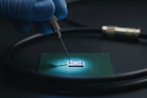
Keysight Technologies and WIN Semiconductors have introduced a joint MMIC design workflow to help gallium nitride (GaN) MMIC designers achieve successful tapeouts on the first attempt. The workflow brings together chip-level simulation, 3D layout and verification, and evaluation board design in one environment. It is aimed at companies developing GaN MMICs for applications such as 5G base stations, Wi-Fi access points, satellite systems, and defense radar.
The workflow automates simulation, optimization, and verification tasks before a design is sent for fabrication. By ensuring all required design checks are completed, it helps reduce the need for costly and time-consuming foundry respins caused by failed tapeouts.
The platform also allows engineers to design and optimise both the MMIC and its evaluation board at the same time. This includes the chip, package, PCB, and test connectors, helping ensure the finished hardware meets performance targets during testing before customer deployment.
The workflow is supported by WIN Semiconductors’ NP120P GaN Process Design Kit, which provides process models and layout rules. Integrated with Keysight’s Advanced Design System (ADS) and RF Circuit Simulation Professional, these models streamline the complete MMIC design flow from simulation through tapeout.
Richard Kuo, Director of Design Service, WIN Semiconductors, said: “We are delighted to collaborate with Keysight to deliver a customized LVS solution within the WIN ADS PDK. By combining Keysight’s ADS expertise with WIN’s robust PDK and advanced process technology, we provided a comprehensive verification solution that streamlined the customer’s design flow and accelerated the time-to-market for advanced RF products with greater confidence and reliability.”
Nilesh Kamdar, General Manager, EDA, Design Engineering Software, Keysight, said: “WIN’s complete PDK, combined with Keysight’s simulation and verification tools, gives designers a single path from chip design through evaluation board. Design houses can now prove full system performance before fabrication, giving their customers the confidence to commit.”
Click here for the original announcement.