




Automated screening and fabrication of two-dimensional semiconductors enable faster materials discovery, reveal thickness-dependent performance and support development of efficient AI chips.
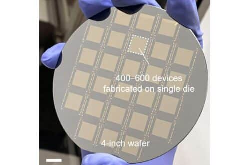
The Korea Advanced Institute of Science and Technology (KAIST) has developed an automated screening and fabrication platform for two-dimensional semiconductors, with findings published in Advanced Functional Materials. The technology could accelerate the discovery of low-power semiconductor materials for artificial intelligence chips by replacing labour-intensive manual analysis with a data-driven workflow.
Two-dimensional semiconductors, which are only a few atomic layers thick, are considered promising candidates for next-generation electronics because they can operate with lower power consumption than conventional silicon-based devices. However, identifying suitable semiconductor flakes and fabricating test devices has traditionally required researchers to manually examine samples under microscopes and individually design electrodes, making large-scale analysis impractical.
Led by Professor Jimin Kwon, the research team developed an automated system that identifies molybdenum disulphide (MoS₂) flakes from optical microscope images by analysing RGB brightness values that vary with material thickness. The platform then automatically designs and fabricates transistor devices, creating a continuous workflow from material identification to electrical testing.
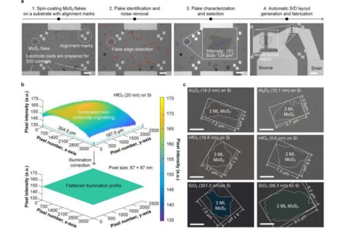
The automated approach enabled researchers to screen more than 120,000 semiconductor flakes, fabricate 1,615 transistors and analyse their electrical characteristics. Atomic force microscopy confirmed that the system could accurately distinguish subtle thickness differences between three and eight atomic layers.

The large-scale dataset also revealed a previously difficult-to-confirm relationship between thickness and transistor performance. As semiconductor layers became thicker, electrical current flowed more easily, but the ability to switch devices on and off declined. The researchers said this trend had remained unclear because earlier studies relied on relatively small sample sizes.
Beyond improving laboratory efficiency, the team believes the platform shifts two-dimensional semiconductor research towards data-driven materials discovery. The automated workflow could help researchers identify high-performance materials more rapidly while supporting future efforts in which artificial intelligence assists in designing next-generation low-power semiconductors for advanced electronic applications.


