


Can 2D semiconductors replace silicon? A new pilot line targets 5nm-equivalent chips without relying on EUV lithography by 2029.
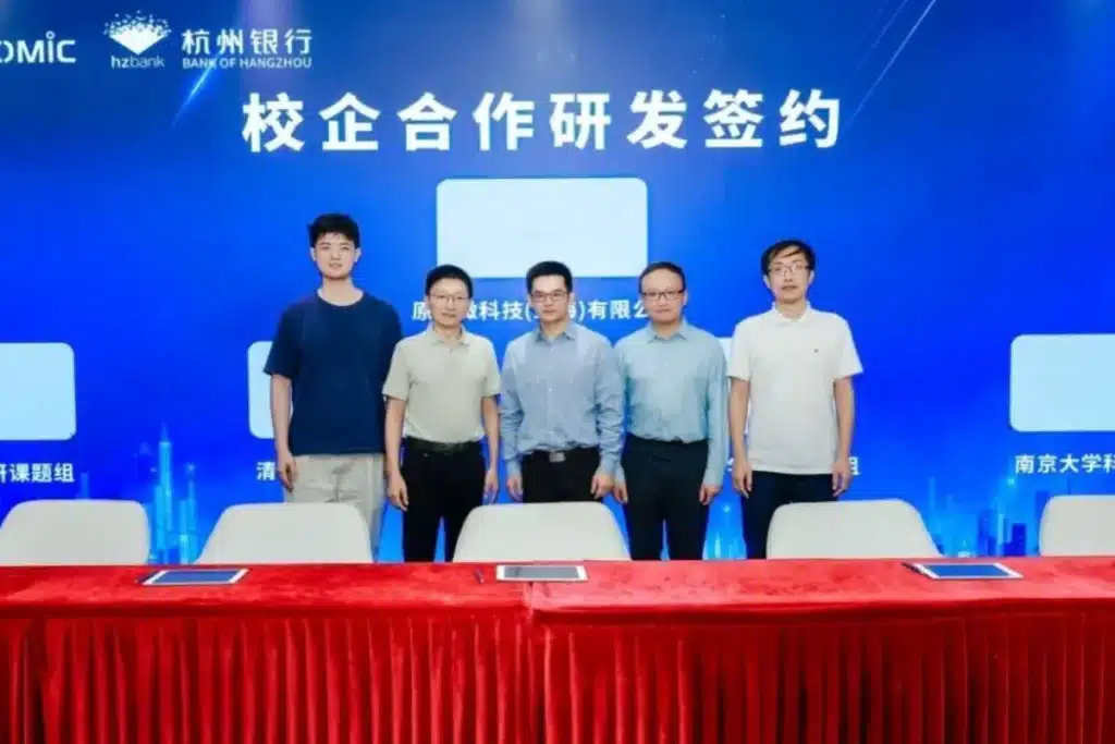
Shanghai-based semiconductor start-up Yuanjiwei has unveiled what it describes as the world’s first 8-inch pilot production line for two-dimensional (2D) semiconductors, designed to support the complete chip manufacturing process from material preparation to device integration and tape-out. The company says the facility will be used to develop 5nm-equivalent chip technology without relying on extreme ultraviolet (EUV) lithography.
Unlike conventional silicon-based devices, 2D semiconductors use atomically thin materials that enable transistor scaling without increasingly complex three-dimensional transistor architectures. Their ultra-thin structure is also expected to reduce leakage current, lowering power consumption and heat generation as devices continue to shrink. The company says these characteristics could also complement advanced packaging technologies such as 3D stacking to improve memory density and overall chip performance.
The pilot line integrates multiple stages of the manufacturing workflow, including 2D material synthesis, wafer processing, device fabrication, chip integration and tape-out. According to Yuanjiwei, bringing these processes onto a single production platform is intended to move 2D semiconductor research beyond laboratory demonstrations towards engineering validation and pilot-scale manufacturing.
The company plans to establish a process comparable to a 90nm silicon node later this year before progressing towards a 5nm-equivalent manufacturing process by 2029. It says the approach could reduce dependence on EUV lithography by exploiting the electrical properties of atomically thin semiconductor materials rather than relying solely on continued transistor miniaturisation.
Although 2D semiconductors remain at an early stage of commercial development, they are being explored by researchers worldwide as a potential alternative to conventional silicon scaling. Their long-term adoption will depend on advances in materials engineering, process integration, manufacturing yield and compatibility with existing semiconductor fabrication technologies.